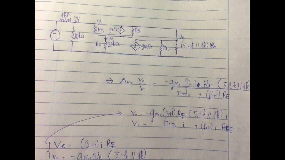
i've been trying to draw the small signal equivalent circuit. And this is what i have
 but i feel something's wrong because when i calculate voltage gain i dont have to use gm of the BJT. can you guys show me where did i do wrong?
i've been trying to draw the small signal equivalent circuit. And this is what i have
 but i feel something's wrong because when i calculate voltage gain i dont have to use gm of the BJT. can you guys show me where did i do wrong?
Your small-signal equivalent circuit is wrong. In your sketched circuit you connected the mosfet's drain to the bjt's collector and the mosfet's gate to the bjt's emitter.
To draw a small-signal equivalent circuit you should substitute each device with its small-signal equivalent, respecting the position of the terminals.