3
\$\begingroup\$

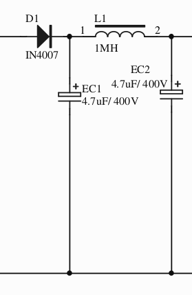
On the left of the circuit shown below is a 120V AC current. I know that the diode (D1) rectifies the signal so that only the positive half of the AC signal goes through.

enter image description here

I have seen circuits with a Diode, L1 and EC2, but with EC1 left out that acts as an half-wave rectifier.

So my question is as follows:

  • Is the output at node 2 a perfect DC signal?
  • What is the voltage of the DC signal if the original AC signal has a voltage of 120V?
  • Am I correct that EC2 keeps the voltage supply to node 2 constant and that L1 keeps the current supply to node constant?
  • What is the purpose of EC1? If it is the same as EC2, why is it not in parallel with EC2 after the inductor?

Note: This is not a homework question. I am brushing up on my knowledge about circuits and came across this as part of a design of a power PCB.

\$\endgroup\$
8
  • 1
    \$\begingroup\$ You can do the simulation yourself with either LTSpice or the circuit simulator that's built-in to this website (ctrl-m in an answer below) \$\endgroup\$
    – scld
    Commented Jul 20, 2016 at 15:40
  • \$\begingroup\$ Thanks for the suggestion, I will definitely try that. However, a simulation will only answer the first two parts of my question and not the last 2 parts. Thanks. \$\endgroup\$
    – user41391
    Commented Jul 20, 2016 at 15:45
  • \$\begingroup\$ Actually, attach a load and it will. \$\endgroup\$ Commented Jul 20, 2016 at 15:47
  • 1
    \$\begingroup\$ Is that really a mega-Henry inductor? \$\endgroup\$
    – pjc50
    Commented Jul 20, 2016 at 15:52
  • 1
    \$\begingroup\$ @Coffee: That was probably a hint that mH would be much more likely. Capitals matter. \$\endgroup\$
    – Transistor
    Commented Jul 20, 2016 at 15:56

2 Answers 2

2
\$\begingroup\$

I'll give a general overview.

1) The output voltage should be ideally constant if you provide perfect filtering (which isn't realistic). Think of \$L_1\$ and \$EC_2\$ as a low pass \$LC\$ filter, that what it is.

2) If your input is a \$120V_{ac}\$ voltage signal, then, after some cycles \$EC_1\$ will get charged up to the peak value of that signal \$V_{peak}=120V(\sqrt2)\approx170V \$. Minus the drop across the diode.

3) Yes. A relatively large inductor keeps current constant (e.g choke inductor) and a relatively large capacitor behaves as a voltage source.

4) Don't think of \$EC_2\$ separately. Along with \$L_1\$, it forms a low pass filter which reduces the ripple on the output signal.

\$\endgroup\$
1
\$\begingroup\$

Let me further elaborate from Sixto's well composed answer:

  1. Is the output at node 2 a perfect DC signal?

This depends on what you mean by "signal". You do not show a load or output current in your schematic. If there is no current being drawn from the output (i.e. from Node 2 to Ground/Common), the output voltage will be a perfectly flat line if you view it on an O-scope. That is, it will have no AC ripple voltage whatsoever. So, yes, I'd call that a "perfect DC signal". On the other hand, if there is a load attached, the output voltage will exhibit an AC ripple voltage riding on a DC level. The heavier the load (less Ohms) the greater will be the AC ripple voltage. Even at such a greater load, the output voltage will still have a DC component.

  1. You are not quite correct in this statement because a portion of the current thru L1 flows into EC2 when the diode is conducting, the other portion flows into the load during this same period of diode conduction. When the diode is not conducting, current flows directly to the load from EC2 and also from EC1 via L1 into the load. Putting actual numeric values to these time-varying currents & voltage is very difficult to do with manual mathematics. However, with modern analysis tools like Spice, it is easy once you know how to use the tools.

  2. The word "purpose" is a bit troublesome here. This type of half-wave filtered rectifier circuit has been around for 100 years. You will find it in several different forms: A: the diode and only EC1, B: the diode plus L1 & EC2, C: as it is shown here with one L and two caps. Each iteration from "A" to "C" adds some benefit to the performance at the expense of more components, and thus more space, more weight and more cost, and less reliability. Circuit designers will pick one of the three common topologies based in the tradeoffs of size, cost, etc. So that if there is a "purpose" to including EC1, it is because it will provide better performance to the overall circuit when analyzed as a whole, not that it adds one specific magic ingredient or segregated benefit.

\$\endgroup\$
0

Your Answer

By clicking “Post Your Answer”, you agree to our terms of service and acknowledge you have read our privacy policy.