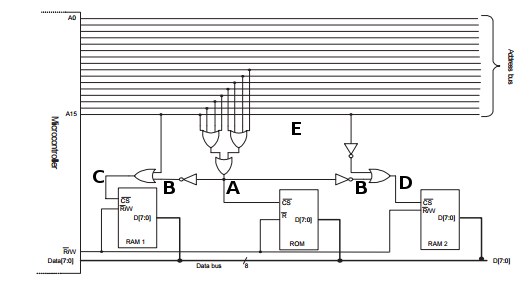
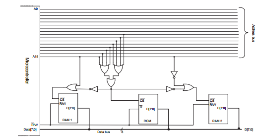
Let's start by labelling some bits of the diagram for easy reference:

Now we can define what the different labels mean.
- A is HIGH if any of A8-A15 are HIGH.
- B is NOT A
- C is HIGH if either B or E (which is A15) is HIGH
- D is HIGH if B is HIGH and E is NOT HIGH.
- E (as I mentioned) is A15.
So we can make some boolean expressions now:
- A = A8+A9+A10+A11+A12+A13+A14+A15
- B = ¬A
- C = B+E
- D = B+¬E
Expanded:
Since CS is always active LOW you are interested in the FALSE values of those expressions - the values that make the expression result in an answer of FALSE.
So if any of A8-A15 are true then A must be true, ergo to get A to be false NONE of A8 to A15 can be HIGH. So A will be LOW for address range 0b00000000XXXXXXXX (or 0x0000 - 0x00FF)
If either B or E are true then C is true. Therefore B and E both have to be false for C to be false. E is A15, so we know now that A15 must be LOW to ensure that C can be false. A has to be true since it is negated to form B. So one of A8-A14 must be high to make A true and thus B false.
That leads us to the address 0b0YYYYYYYXXXXXXXX where at least one of Y must be high and we don't care about X. That is, anywhere between 0b00000001XXXXXXXX and 0b01111111XXXXXXX, or in hex: 0x0100 to 0x7FFF.
D is the same as C except for the fact that E is inverted. That means that A15 must be HIGH to make D able to be false. Since A15 is high we have the ability to set A8-A14 low and still be valid for this range. So we get 0b1YYYYYYYXXXXXXX, or 0b10000000XXXXXXXX to 0b11111111XXXXXXXX, or in hex: 0x8000 to 0xFFFF.
To put those address ranges in context let's build a full memory map:


