0
\$\begingroup\$

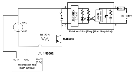
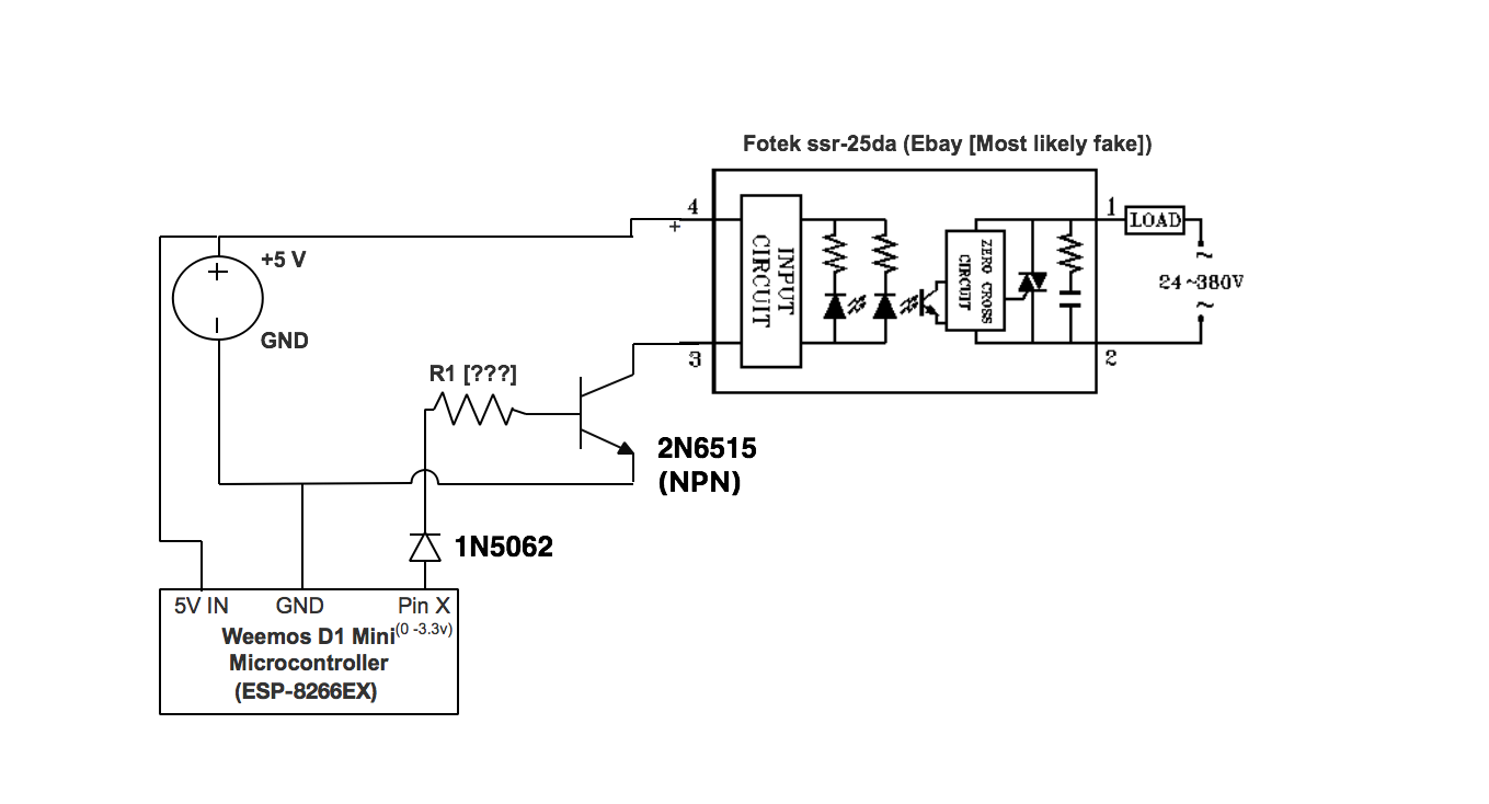
I have recently started medelling in the understanding of circuitry and have started creating this project. As i bought the SSR from eBay i strongly suspect it is a fake and will probably not handle 25A of current nor be as safe as the official data sheet states [Even with an optocoupler]. Now to fully let my heart rest i tried to design this basic protection circuit, but have been hitting a wall with the answer to how to calculate a resistor to limit current and voltage at the base of the transistor. I have googled around for a long time now and still can't seem to figure this out so any help would be appreciated. :) enter image description here

Here are links to the specific data-sheets :

http://pdf1.alldatasheet.com/datasheet-pdf/view/4856/MOTOROLA/MJE350.html (MJE350)

\$\endgroup\$
4
  • 2
    \$\begingroup\$ Conventions in circuit diagrams, + rail at top - or ground at the bottom. The diagram you have put up makes no sense please go back and try to redraw it. \$\endgroup\$
    – RoyC
    Commented Dec 31, 2016 at 21:44
  • 1
    \$\begingroup\$ It should be noted that if the SSR you bought is 'unsafe' in any way, none of the suggested circuits (so far) will make the slightest improvement. For example, if the isolation fails it could certainly take out your ESP and quite possibly a computer etc. connected to it, and/or cause a serious shock hazard. \$\endgroup\$ Commented Dec 31, 2016 at 23:37
  • \$\begingroup\$ While the Fotek range of products seems to be cheaper and Chinese made you tend to get what you pay for. If it's ultra cheap it may well be fake product. However, you design solutions for original product, why would you design solutions to handle a 'fake' when you don't know what about it is fake? Perhaps the fakes only use under rated Triacs: ul.com/newsroom/publicnotices/… or this: instructables.com/id/… ...what circuit mods would you do?? \$\endgroup\$ Commented Jan 1, 2017 at 5:38
  • \$\begingroup\$ Thats what i was intending with fake. I have specifically read about multiple cases of a 12A triac being used and or not complete coverage by the internal resin they use. Other than that i know that the build quality is pretty okay. Just sadly as i cant really open the relay without destroying it then i though that trying to create an extra layer of "protection" (now i understand it really wasn't) seemed like a good idea. \$\endgroup\$
    – user134640
    Commented Jan 1, 2017 at 10:40

2 Answers 2

5
\$\begingroup\$

Rather than just send you away with criticism of what you do or don't know, let's work through your problem and help you learn something.

Clearly you have a microprocessor with an output pin and you want to turn on/off an SSR. Whether it's fake or not is beside the point. You can learn much from it's somewhat sparse datasheet.

The block diagram tells you the basics of the switch:
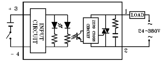
enter image description here

...and here I've corrected the diagram so some won't get upset at not using conventions for voltage and I/O in a schematic.

Let's deal with just the drive requirements for the moment. From the datasheet:
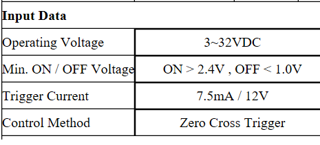
enter image description here

From this you can within reasonable limits work out how much drive current is required to turn on the SSR.
The switch drive is optically coupled to the output side, and you can see there are actually two LED's used (and they are almost invariably IR/Red with a forward voltage about 2.2 V).
Given the datasheet defines the current as 7.5 mA @12 V input, we can get a rough idea of the resistor values. (12 - 2.2)/0.0075 --> 1.3k Ohm ...we can't establish what the value is for each since we don't know how much current flows in each LED, but we can now decide how much current would flow when driven by a 5 volt input signal. (5 - 2.2)/1300 --> 2.1 mA (approximate).

From this low current at 5 V we can deduce that you don't need a drive transistor at all since most microprocessor I/O pins will typically support > 10 mA. But we'll deal with your actual microprocessor later.
So you can drive this switch directly with no transistor and no series resistor from a 5 V supply.

Note: My guess is that the drive is unevenly set between the visible status LED and the optocoupler LED, so it may be that the status LED is barely visible at 5 V drive.

It appears that your microprocessor board is a Wemos D1, and from it's datasheet this is a 3.3 V device. The board has a 5 V to 3.3 V regulator on it, but all the I/O signals are 3.3 V.

Since your microprocessor is 3.3 V, you will actually be able to drive the switch directly. While you are very close to the minimum 3 V specification from the datasheet, notice that they actually break out separately and specify 2.4 V as the absolute minimum on voltage.

However if you are nervous about temperature ranges etc, then it can be wise to provide a higher level of drive, so your original thought of a transistor drive is quite valid. However we now know the current requirements are very small when driving the switch input from 5 V so you could use almost any general purpose TO92/SOT23 NPN switch to do this task.

Lets choose a 2N2222 which has more than enough current sink capability for our task and is cheap ($0.03).
IC is 2.1 mA in this application and the 2N2222 has min Hfe of 50 @1 mA. So the base current required is approximately 0.0021/50 --> 42 uA (a poofteenth).

We can essentially ignore this base current requirement and simply set an overdrive level we are comfortable with. From the ESP8266 datasheet the I/O pins are able to sink/source 12 mA. If we set the base current to 1 mA @3.3 V then we have a series resistor of 3.3k Ohms.

So the final circuit looks like this:

schematic

simulate this circuit – Schematic created using CircuitLab

Hope this helps.
\$\endgroup\$
3
\$\begingroup\$

It's not clear what you are trying to do, but there are some obvious problems with this circuit:

  1. The power to this Weemos thing (whatever it is) seems to be backwards. The "5V IN" terminal it connected to ground, and "GND" is connected to 5 V.
  2. The high power voltages at bottom, instead power rails sorted in decending voltage order down the page, makes the schematic confusing to look at.
  3. Curent flows out of the base of PNP transistor. The diode prevents that.
  4. I can't guess what purpose you think the diode is intended to serve.
  5. The emitter of the transistor is tied to 5 V, but the signal is 3.3 V as implied by the "Pin X (3.3V)" label for the terminal. To be useful, this must be a signal, but the terminal name implies something else. If it really is a signal and its high level really is 3.3 V, then the transistor will always be on at least a little. It would be better if the signal and power voltages were the same.
  6. I don't know what the switch in series with a capacitor (or is that a battery?) is supposed to do.

Step back and explain what you really want to accomplish, and leave your imagined solution out of it. It's easier to answer a question when bad assumptions don't have to be dispelled first.

\$\endgroup\$
2
  • \$\begingroup\$ Im sorry about the shitty drawing. I will redraw it hopefully to make it at least 50% more understandable \$\endgroup\$
    – user134640
    Commented Dec 31, 2016 at 22:55
  • \$\begingroup\$ +1 Good way to start the new year (1224 (ie pm) on 1-1-17 here) - or end the old one there. That question could easily have been treated "differently" :-). Keep it up. (And don't worry - there's minimal risk of ending up being like me :-) ). \$\endgroup\$
    – Russell McMahon
    Commented Dec 31, 2016 at 23:23

Your Answer

By clicking “Post Your Answer”, you agree to our terms of service and acknowledge you have read our privacy policy.

Not the answer you're looking for? Browse other questions tagged or ask your own question.