It's been long enough. You haven't added that much, but I suppose it is more because you have no clue about where to start. I suspect I also don't have a clue, so you really shouldn't feel badly about this. As you will see by the end, I don't think the problem can be solved well.
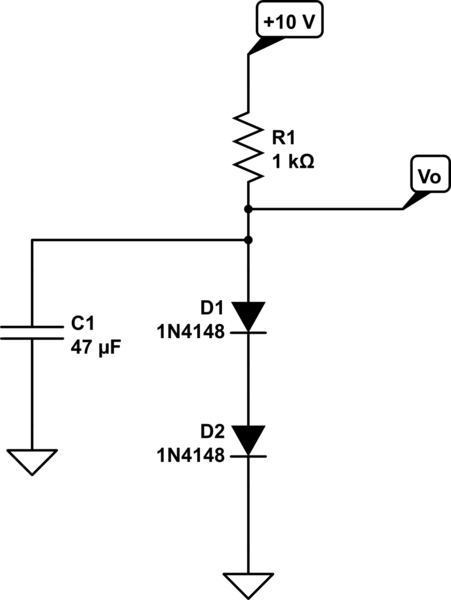
I'll start with the special case discussed in the problem statement, the use of two diodes as a voltage reference. This simply means something like this:

simulate this circuit – Schematic created using CircuitLab
The diodes above are stacked in series. There's a reason for this that will become clear, later. Otherwise, the idea here is to supply a fixed current through the diodes, which causes a voltage drop across them. If you can keep that current fixed, then the voltage across the pair should remain consistent. The capacitor is added to help stabilize that voltage and to reduce voltage noise. (It's not strictly necessary, though.) The resistor is a poor-man's source of current. You are supposed to make a source of current (or a sink) and to get there you may be permitted to use a simpler current source like a resistor. The resistor's ability to keep a consistent source of current is modest. The greater the voltage across it, compared to the voltage across the diodes, the better it works for you. But in this example, it's probably good enough. It has almost \$9\:\textrm{V}\$ across it and slight voltage variations across the diode pair won't affect the current enough to worry about it. You could nearly double that, by tying the cathode end of \$D_2\$ to \$-10\:\textrm{V}\$, but the improvement (twice) isn't important enough to care that much. And it makes something else that will become more important degrade. So I'd probably go this way as a good compromise.
Now, you need to add the BJT. Or two. Or three. Or more. The problem doesn't state. Given that freedom, any manner of answers can arrive -- all the way to a complex design fit for an IC. But let's go with one BJT, for now.
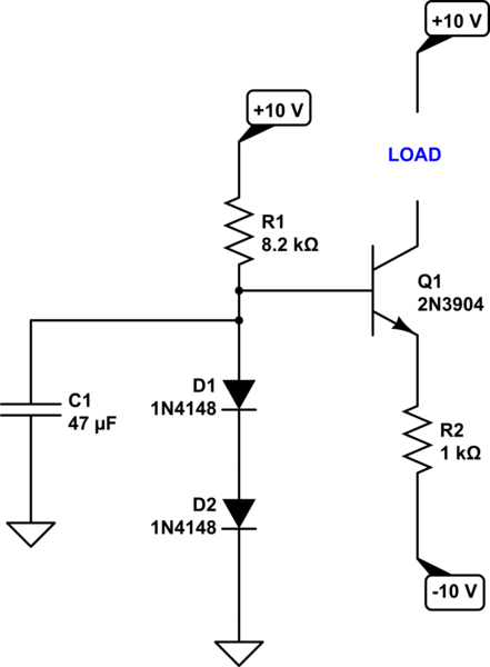
The idea is to hook the base of the BJT to \$V_O\$ and let the emitter fall about one diode drop below the base. The emitter should remain at a fairly consistent drop relative to \$V_O\$, which is actually a quite useful fact. Now you can simply hang a resistor from the emitter to \$V_{EE}\$ like this:

simulate this circuit
Here, the collector has to have almost exactly the same current as the emitter. Since the emitter is at a relatively fixed voltage, too, we can estimate the current in \$R_2\$ and this must be the emitter current. Given \$\beta=100\$, I can estimate the base current at \$\frac{10\:\textrm{mA}}{\beta=100}\approx 100\:\mu\textrm{A}\$. This means \$R_1\$ should supply at least \$10\times\$ that amount, or about \$1\:\textrm{mA}\$. I've adjusted the value of \$R_1\$ to approximately do that.
The value of \$R_2\$ is estimated by first guessing the silicon diode voltage drops at \$I_D=1\:\textrm{mA}\$. I will just use \$700\:\textrm{mV}\$ each. So the voltage at the base of the BJT is \$+1.4\:\textrm{V}\$, by assumption here. I also estimate the \$V_{BE}\$ drop of the BJT to be \$700\:\textrm{mV}\$, as well. This puts the emitter at \$+700\:\textrm{mV}\$. Given the extra \$10\:\textrm{V}\$ needed to get to \$V_{EE}\$, I figure about \$10.7\:\textrm{V}\$ across \$R_2\$. The base current is estimated to be \$100\:\mu\textrm{A}\$, so the emitter current must be \$I_E=100\:\mu\textrm{A}+10\:\textrm{mA}=10.1\:\textrm{mA}\$. This means \$R_2=\frac{10.7\:\textrm{V}}{10.1\:\textrm{mA}}\approx 1.06\:\textrm{k}\Omega\$. As you can see, I used a nearby standard value. The collector current will be a little high. But this may be okay for your use.
Now, let's discuss \$h_{oe}\$. It defines what amounts to the conductance of a resistor across the collector/emitter terminals of the BJT. The value you were given is unusually large. But there it is. The current through it will be \$h_{oe}\cdot V_{CE}\$ and this adds to the collector current. This means there will be a load-dependent variation in the current through the load that degrades the performance. But that value of \$h_{oe}\$ is very unusual. It is normally at least three orders of magnitude less than that. The value you were given is ... well, insanely bad.
It's so bad that with a low-valued resistance as the load, \$V_{CE}\ge 10\:\textrm{V}\$ and therefore the current through this bypass can be as much as \$10\:\textrm{V}\cdot h_{oe}\approx 37\:\textrm{mA}\$. That won't actually predict things since the whole idea is a mess. But it does say that the value you were given for \$h_{oe}\$ means the above circuits can't be made to behave in any useful way.
Let's predict the behavior. \$h_{oe}\$ implies a resistor between collector and emitter of \$R_{hoe}= \frac{1}{h_{oe}}\approx 270\:\Omega\$. If the load is \$0\:\Omega\$ then this suggests a maximum current through the load of about \$15.75\:\textrm{mA}\$. So it's not really as bad as \$37\:\textrm{mA}\$ because you will never be able to get \$V_{CE}\ge 10\:\textrm{V}\$, but more like less than half that. Which is why the maximum current is lower, by half. The BJT will stay pretty much OFF until the load increases its resistance to the point where the emitter of the transistor can sink down towards \$V_{EE}\$ such that it can turn ON. This will happen when the load resistance reaches about \$1\:\textrm{k}\Omega\cdot\left(\frac{20\:\textrm{V}}{10.7\:\textrm{V}} -1\right)-270\:\Omega\approx 600\:\Omega\$. Once that point is reached, the BJT can start to turn ON and do something. (Just before this point, the load current rises to about \$10.7\:\textrm{mA}\$.)
But as the load resistance increases, the BJT goes rapidly into saturation and starts drawing huge currents from its base. This will rob the diode current, suggesting making \$R_1\$ a lot smaller to compensate (but no point as the whole idea is insane.) The BJT will finally become a "switch" across \$R_{hoe}\$ when \$V_{CE}\$ declines to about \$400\:\textrm{mV}\$ and that will happen when the load resistance climbs to about \$1\:\textrm{k}\Omega\$. This means the transistor is doing something for a load from only about \$600\:\Omega\$ to about \$1000\:\Omega\$.
Again, we've determined that the whole idea is close to useless. Barely an improvement over just using a resistor to limit the current.
One way to try and fix that problem is to go to a cascode design in order to limit \$V_{CE}\$ variations on the BJT. But this isn't of any use because, if you have to use the same crappy BJT for this new cascoding BJT, it's going to have the same problem. So the idea really can't be fixed that way.
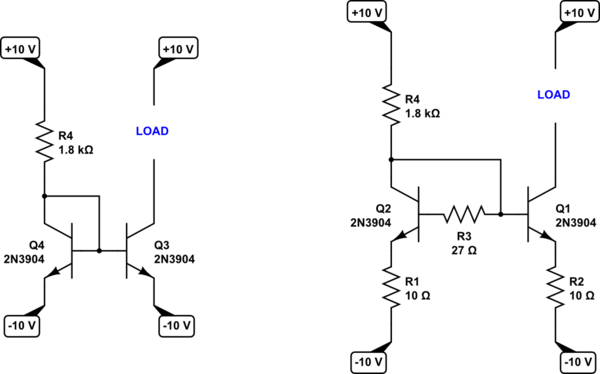
Assuming you could find a matched pair of BJTs, ones that are this bad I mean, then you could use a current mirror. This looks more like one of the following:

simulate this circuit
The left side is the usual simplistic form. The right side deals with variations in \$\beta\$ and \$V_{BE}\$ in real world BJTs. (Yours aren't.) However, none of this really works either because of your huge \$h_{oe}\$. Adding more BJTs won't really help. Your crappy BJTs effectively have a low-valued resistor across their collector-emitter legs with such a low value against such high supply voltages and modest load current goals by comparison, that I think your problem is probably mis-stated. Typical values of \$h_{oe}\$ are many orders of magnitude lower.
Let's look at a datasheet. Try this one: OnSemi's PN2222A. Here on page 3 you will see that with \$I_C=10\:\textrm{mA}\$, \$25\:\mu\textrm{Mhos}\le h_{oe}\le 200\:\mu\textrm{Mhos}\$. This means \$R_{hoe}\ge 5\:\textrm{k}\Omega\$. (And more likely closer to \$25\:\textrm{k}\Omega\$.) This would make such a design quite achievable within some reasonably approximate behavior relative to the load, itself.
But your specs just make the whole idea relatively crazy without a load resistance specification, which is lacking here. (If you knew the load and the load itself had a narrow range, then it might be possible to center the design using these lousy BJTs so that there was some modest range of control. But you don't have that specification.)
The upshot here is that suggestions about current mirrors, or any other approach, are likely doomed. I don't think there is a good suggestion for you. I'm not even sure there is a usable topology. But if there is (and I'm not excluding the idea, entirely, as that would require examining every possible arrangement constrained only by the problem statement as well as predicting the future of all human imagination here), I'm sure it would be a rather complex design.


