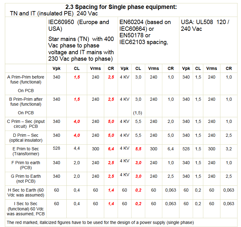
I've read a whole bunch of material but I'm still quite confused regarding creepage clearance, specifically:
How to calculate the minimal clearance on a PCB board?
How to calculate the width of the air gap (pcb cutout, hollowed slot of pcb) to enhance clearance should you really, really not be able to meet the minimum clearance in question #1 and decide to use air gap instead?
Elaboration:
Based on what I've read, for 300Volts WORKING circuit, the minimum clearance is expected to be 3.2mm, so I assumed, since my working voltage is 220v and maximum input voltage is 305v, a 3.3mm clearance will suffice. But according to this online calculator (http://www.creepage.com/) the minimum clearance is only 2.1mm (I could have remembered it wrong in which case I apologize) so how should I actually crunch the numbers?
I also heard that UL test labs will tune the input all the way to 2kv, sometimes higher (though I don't know for how long), and apply it to your board and your board have to survive without giving out sparks or outright be reduced to nothing but a charred wreck. This further perplexed my understanding of the minimal clearance: there is no way I can cater 2kv???
My board is tightly packed and some places really can't enable me to afford the 3.3mm luxury, which bring us to question #2, how wide should I make the air gap to offset the negative effect of the small distance? Is there a way to calculate that too?
This is really all too overwhelming as there are just too much information to process. So what would be the general rule of thumb, speaking particularly from experience?
BTW my pollution level is 2.

