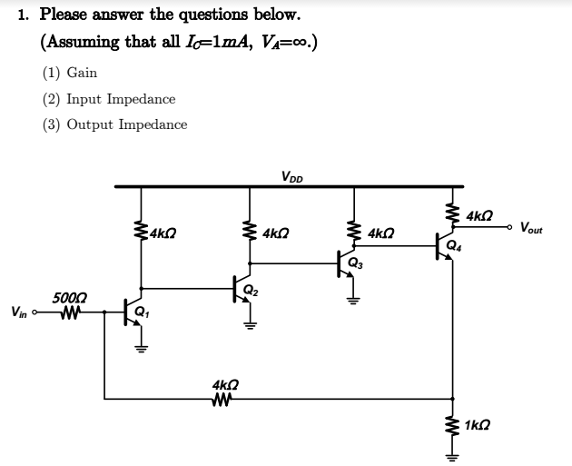
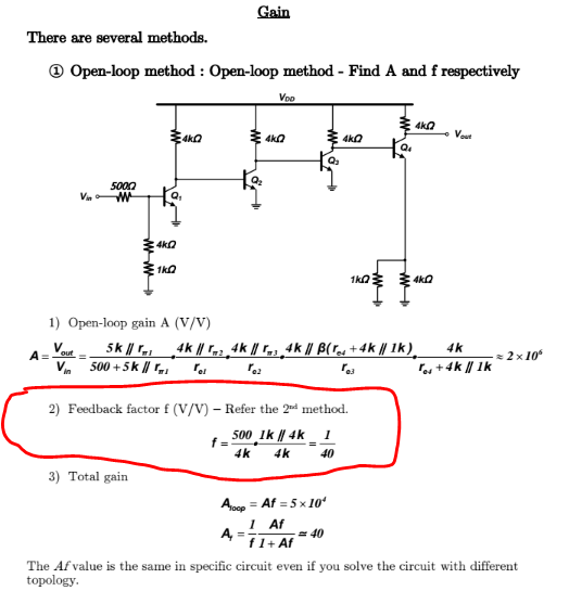
Below is an exercise with solution about feedback network. I am wondering how the feedback factor is calculated like that. Could anyone shed some light on this?
-
1\$\begingroup\$ 4000/500 = 8, just like an op-amp with negative feedback. This makes input Z = 500 and of course output Z is rE of the final transistor which is going to be somewhere between 10 ohm and 30 ohm. In other words, I'm past the point where I care to do precise computations on circuits like this LOL. \$\endgroup\$– Andy akaCommented Jun 12, 2017 at 11:57
-
1\$\begingroup\$ And I've just noticed in your question that Ic = 1mA hence rE will be 26 ohms (26mV/Ic). Va is infinity (in your question) hence the gain will be 8. I can make this an answer if you want. \$\endgroup\$– Andy akaCommented Jun 12, 2017 at 12:51
-
1\$\begingroup\$ Regarding the feedback factor: f=Vbase/Vout for Vin=0. \$\endgroup\$– LvWCommented Jun 12, 2017 at 14:45
-
1\$\begingroup\$ Regarding the feedback factor: f=Vb1/Vout for Vin=0. Assuming rbe1=h11=hie1=5k (Ic=1mA) we can calculate Ve4=ic*0.8k and Ve4/Vout=0.8k/4k. From this, f=Vb1/Vout=(4.45/8.45)0.8k/4k. So we arrive at a feedback factor of app. f=0.1. \$\endgroup\$– LvWCommented Jun 12, 2017 at 14:57
-
1\$\begingroup\$ More than that - I doubt if the shown method for open-loop gain calculation is correct. \$\endgroup\$– LvWCommented Jun 12, 2017 at 15:35
2 Answers
Gain at Q4 collector is 40.
This can be seen as the the output 4k load is driven by a current source (Q4 collector). Current is found as input current Vin/.5k which flows through the 4k feedback R. Feedback drives emitter of Q4 to -Vin/.5k * 4k=-8*Vin causing the net emitter current to be (Vin)(1/0.5k+(4k/0.5k)(1/1k))=vin*10e-3. Multiply by 4k and divide by Vin to get 40.
Each of the gain stages is 4K/(0.026 / 1mA) = 4K/26 = 150X or 42dB. Total low frequency gain is 126dB (2 Million), ignoring any loading by the next stage's DC rin (probably significant, but no beta is given, so ignore that gain-shunting).
Gain will be Rf/Rin = 8x (14dB). There is a rather effective Virtual Gnd activity, thus Rin sets the input resistance.
DC Rout will be 26 ohms/gain_margin = 26 / (2million/8) = 26/ 250,000 or 0.1 milliohm.
-
\$\begingroup\$ I think, loading of the following stages must not be neglected because the expected rin (rbe=hie) will be in the same order as a the collector resistors. \$\endgroup\$– LvWCommented Jun 12, 2017 at 16:44
-
\$\begingroup\$ correct---but we have no beta data; if same (4K || 4K), the open loop gain remains at 8X, Rin still 500, and Rout increases from 100uOhm to 800uOhm. \$\endgroup\$ Commented Jun 12, 2017 at 16:50
-
\$\begingroup\$ .... "if the output were on Q4 emitter" is missing at the beginning of your answer \$\endgroup\$– carlocCommented Nov 26, 2018 at 17:04


