3
\$\begingroup\$

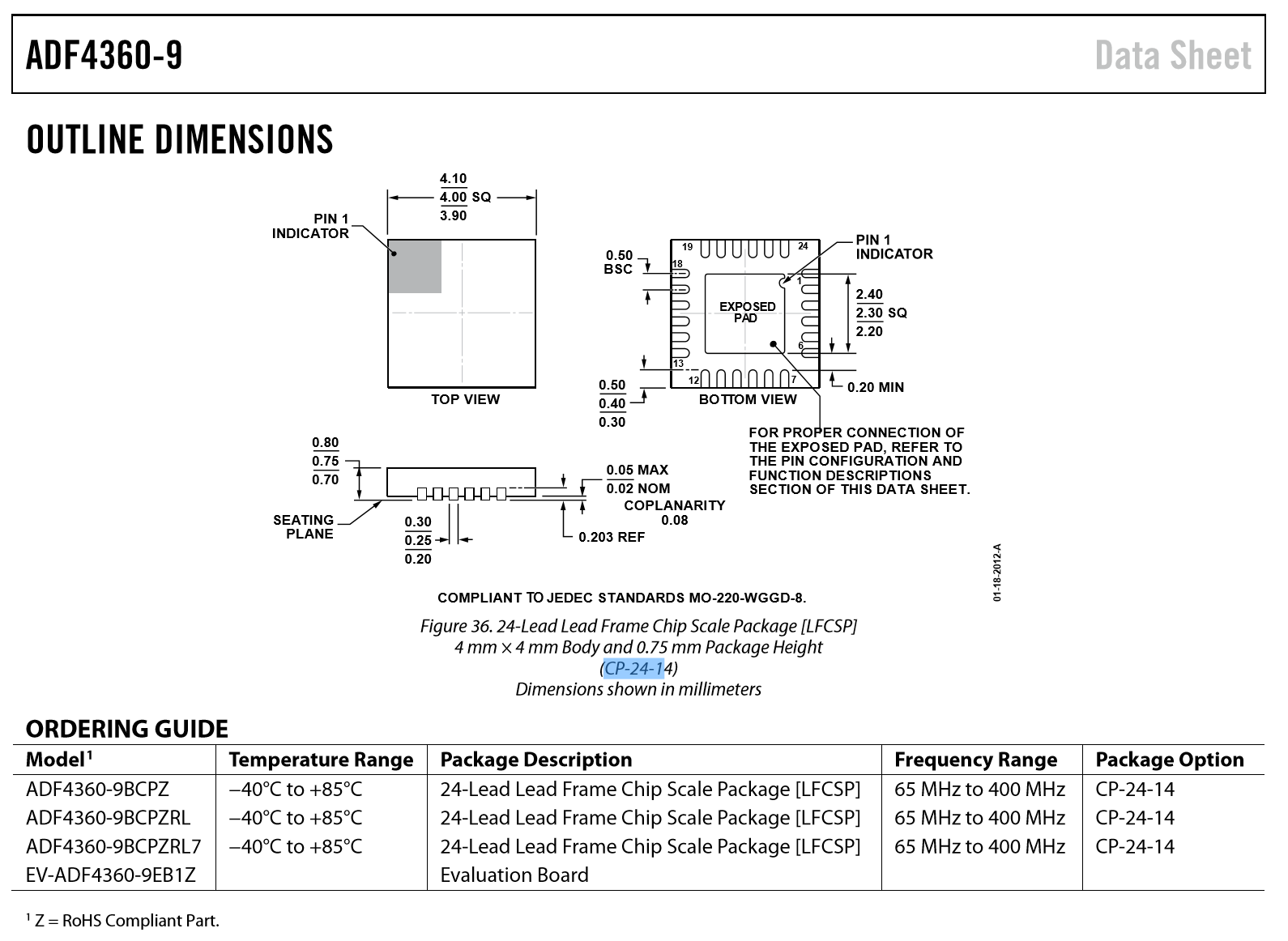
I have the following PCB datasheet, but I am very uncertain as to what it is saying. Some of the dimensions each have 3 numbers, which I took as nominal, minimum and maximum values, however, the sides do not add up.

The datasheet says that each side should be 4mm in length, however, adding up each of the individual components of a side does not add up to 4.

Am I reading this wrong? How would I go about designing a PCB for this?

enter image description here

\$\endgroup\$
2
  • \$\begingroup\$ There is an inconsitency in the dimensions given. If the pads are on 0.50 mm centers, as shown at the top left of the bottom view, the distance between centers of Pin 1 and Pin 6 should be 2.50 mm, not the 2.30 mm shown at the right of the bottom view. \$\endgroup\$ Commented Jul 23, 2017 at 22:17
  • \$\begingroup\$ @PeterBennett, that 2.30 is the size of the center pad. \$\endgroup\$ Commented Jul 24, 2017 at 3:33

3 Answers 3

2
\$\begingroup\$

They aren't giving you the dimensions of all the distances that would add up to 4 because you don't need to know them. They aren't telling to how far it is from the pads to the corner of the package because you don't need to know that.

The process for designing the footprint goes something like this:

With a nice symmetric pattern like this, let's say the center of the part is 0,0.

Let's start with the vertical row of pads on the right.

  1. The dimensions of the pads are given: 0.40 by 0.25
  2. The x coordinate of the outside edge of the pads is given: (4.0/2)
  3. So the x coordinate of the center of that row of pads is the half their length from the outside edge: 2.0 - (0.40/2)
  4. There are an even number of pads, centered vertically around y = 0.
  5. The distance between the centers of the pads is given: 0.50
  6. So the y coordinate of pad just above the center is 0.50/2
  7. Place a pad at that location (1.8,0.25)
  8. Select the pad and use your tool's 'step and repeat' function to create the rest of the pads in that row above and below it, on 0.50 centers
  9. Select the row and use the step and repeat to create the other vertical row. These rows need to be offset by the width of the part minus the length of a pad, so 4.0-0.40.
  10. Repeat this process for the other two rows of pads.
  11. Add the center pad
  12. Check everything.

I will say this: making footprints is one time when it's really worthwhile to either use a pdf reader that allows you to mark up the drawing, or to print out the drawing and make notes with a pencil.

Note that this is assuming you want the pads on the footprint the same size as the ones on the part. This is not always the case.

\$\endgroup\$
1
\$\begingroup\$

The Datasheet doesn't show the footprint details. What you need is the footprint data. If it isn't in the datasheet, then the vendor probably provides it as a separate document. Putting "LFCSP" into the search box of their website:

http://www.analog.com/en/design-center/packaging-quality-symbols-footprints/package-index/csp-chip-scale-package/lfcsp.html

\$\endgroup\$
1
0
\$\begingroup\$

The three numbers for each measurement is the tolerance for that measurement. So the package is 4 X 4 mm, but that is just nominally - in reality the part you buy will vary from 3.90 to 4.10. 4.0 +/- 0.1 mm. This is probably not very important for a low density board where there is a lot of space between this component and it's neighbours, but tolerances stack up, so the closer you place stuff, the more important the outline tolerance becomes. The recommended footprint will typically take in account the dimensional tolerances of the part pins.

\$\endgroup\$

Your Answer

By clicking “Post Your Answer”, you agree to our terms of service and acknowledge you have read our privacy policy.

Not the answer you're looking for? Browse other questions tagged or ask your own question.