0
\$\begingroup\$

I am doing an electronics project that involves transmitting and receiving information on the 915MHz ISM band. I need to make the enclosure as small as possible. However, that means that I don't have a lot of space for my antenna that is tuned for the 915MHz ISM band.

Here is the picture of how it would look like in the enclosure: enter image description here
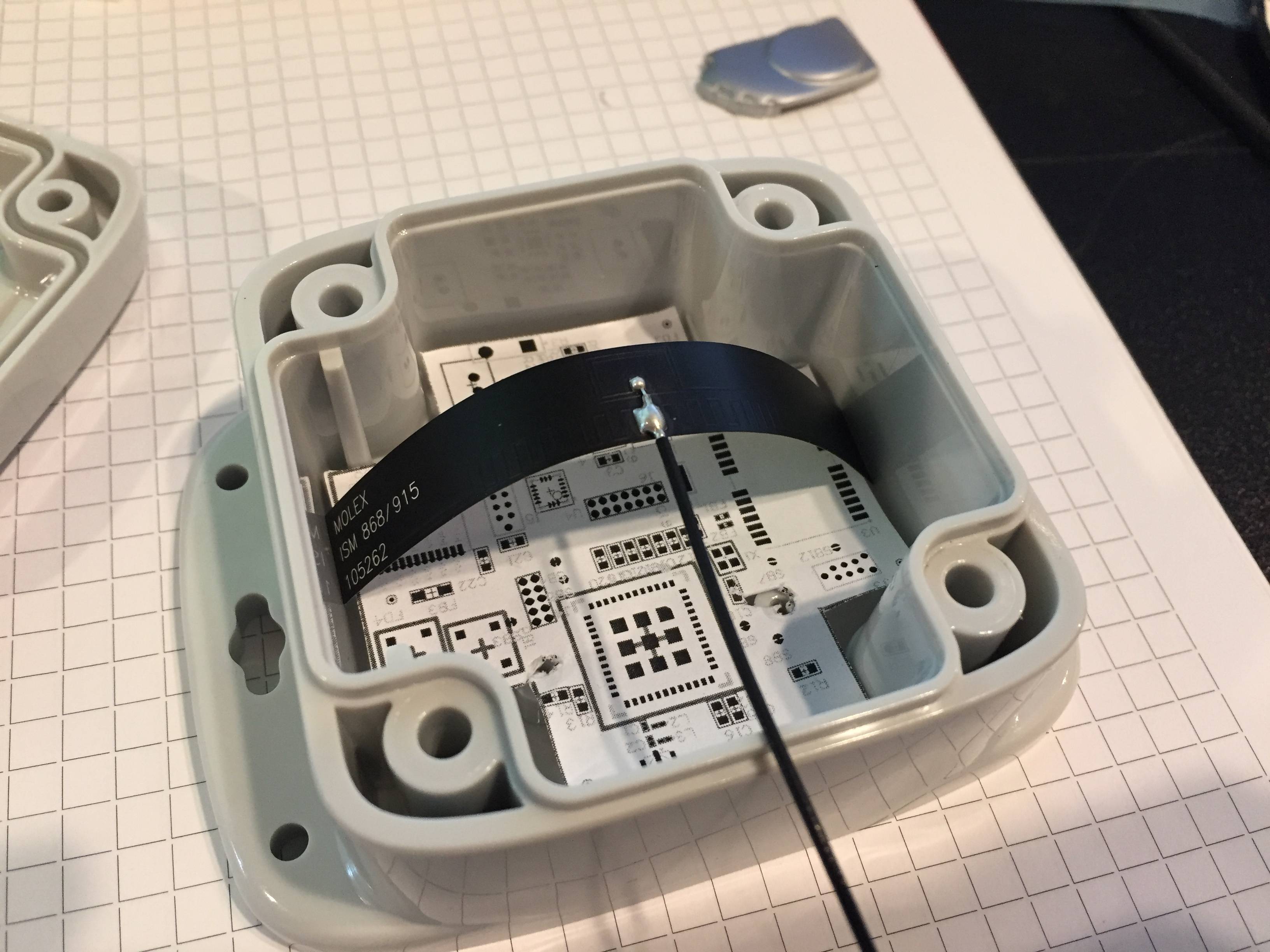
Hwow will the performance be affected by the fact that I am folding the antenna like this? Am I better off just using a helical antenna in this case?

\$\endgroup\$
7
  • \$\begingroup\$ Proximity of end points is sensitive to ground plane, but no design will be ideal, unless to have a particular favoured direction. In this case, radial dipole end views will be the weakest, but since curved, it wont be null. Using a sig gen and SA, you can measure the relative pattern loss in enclosure vs outside. using coax to ground plane. Can you measure return loss? \$\endgroup\$
    – D.A.S.
    Commented Sep 6, 2017 at 21:43
  • \$\begingroup\$ I wish I could, but I don't have a VNA. Maybe I can try with a spectrum analyzer? \$\endgroup\$
    – Alex C
    Commented Sep 6, 2017 at 21:57
  • \$\begingroup\$ Yes you can use any antenna on SA and transmit with a sweep RF and sync FM to SA then use direction coupler for RL. \$\endgroup\$
    – D.A.S.
    Commented Sep 6, 2017 at 22:03
  • \$\begingroup\$ what orientation is preferred for direction? \$\endgroup\$
    – D.A.S.
    Commented Sep 6, 2017 at 22:06
  • \$\begingroup\$ It basically needs to not radiate towards the bottom direction (towards the PCB). This is a LoRa product, I basically just need to communicate to anywhere that has a gateway. \$\endgroup\$
    – Alex C
    Commented Sep 6, 2017 at 22:13

1 Answer 1

2
\$\begingroup\$

The datasheets indicates it should not be closer than 5 mm to the PCB...which you will clearly violate. As a center fed antenna, bending it will change the radiation pattern if you bend it, but you'd have to measure it to find out if it's good enough for your application.

You may have more success with a Triple Band Antenna such as the 209132

\$\endgroup\$
2
  • \$\begingroup\$ That antenna is very interesting, but I am having difficulty understanding the reference PCB design: - Why do you need all the castellations on the side of the PCB? - If I have more than the minimum ground plane area (as seen in the picture I posted), is the design still OK? - Can I still populate the top part layer with components or should the layer over the ground plane be empty of components? Thanks! \$\endgroup\$
    – Alex C
    Commented Sep 6, 2017 at 21:58
  • \$\begingroup\$ The design is all black magic to me.......Once I know where to connect the cable the Antenna is a black box. Do you really need to know the intricacies of the design? \$\endgroup\$ Commented Sep 6, 2017 at 22:30

Your Answer

By clicking “Post Your Answer”, you agree to our terms of service and acknowledge you have read our privacy policy.

Not the answer you're looking for? Browse other questions tagged or ask your own question.