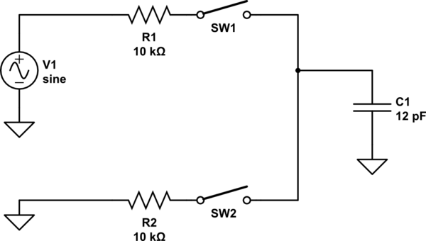
Your circuitry looks like a non-ideal switched-capacitor circuit (due to the 10k resistors). Hence, it can be treated mathematically using digital signal processing tools - provided that
the clock period Tcl is much larger than the time constant of the RC-combination (seems to be fulfilled with Tcl=1E-5>>1E-7=RC),
The period Ts of the input signal is much larger than the clock period Tcl
(Ts>>Tcl, fs<<100kHz).
In this case, your circuit with two switches and the grounded capacitor can be treated as a simple combination of a grounded capacitor and a "toggled" switch (non-ideal with an on-resistance of 10k), which allows capacitor charging during one switch period and discharging during the other period. However, if both above mentioned requirements are fulfilled, the capacitor can be assumed as fully charged/discharged in each clock period - and the value of the resitor (10k) plays no major role.
For such a combination a time continuous linear ac equivalent does exist (based on z-transformation) which was described by B.D. Nelin in 1983 (IEEE Transactions Circuits and Systems, vol CAS-30, pp 43-48).
Such a toggled-switch capacitor block (called "storistor") has the following transfer function in the z-domain: Hz=z*exp(-1/2).
In each simulation programm (ac analysis) this storistor model can be realized using an analog delay element (delay line) with a delay of Td=(1/2)Tcl . The delay line should be terminated properly with a resistor Rl which equals the characteristic impedance of the delay line.
Fazit: For low frequency signals (fs<<100kHz) , the shown combination produces nothing else than a pure delay of the signal.


.TRANfreq sweep from 100 to 1k, with fs=1k, will not give the usual sampled symmetry, but something mingled. I don't know how to represent such an aliasing difference in.AC. Furthermore, as carloc mentions, it is dependent on the duty cycle, if this would be the case. \$\endgroup\$