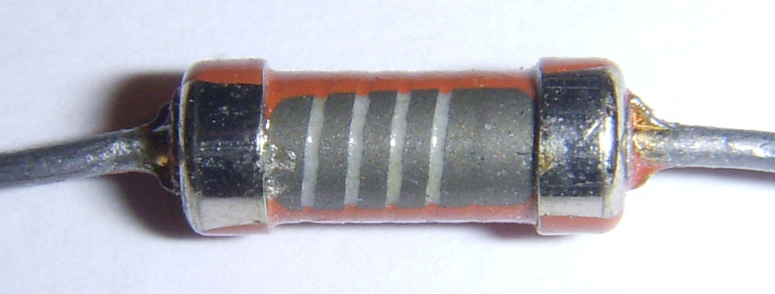
Figure 1. A carbon film resistor. Photo by Shaddack from Wikimedia Commons.
This photo shows the internal construction of an unpainted carbon film resistor. A spiral cut has been made in the film through to the ceramic former. For a given film resistivity a range of resistance values can be created by varying the pitch and width of the cut in the film. This one is a little suspect as all the heat will be dissipated in the high-resistance section where the spiral is so they are not spreading it evenly across the film. Presumably this is taken care of in the design calculations.
Shouldn't the area of resistor also determine its conductivity?
The resistivity and thickness of the uncut material is controllable in manufacture. Then the cutting operation can fine-tune the resistance value.
If you supplied a 1000 watt resistor with 3.3v and 100ma, for instance, would you get the same reading as you would get if you passed the same current through a 1/8 watt resistor?
Only if both are \$ R = \frac {V}{I} = \frac {3.3}{0.1} = 33 \ \Omega \$. The power dissipated in each would be \$ P = I^2R = 0.1^2 \times 33 = 33\ \text {mW} \$ so both would be fine.
Furthermore, if you do get the same reading, shouldn't the area of the larger resistor affect the resistance?

simulate this circuit – Schematic created using CircuitLab
Figure 2. (a) A small 100 Ω resistor and (b) another one that can handle four times as much power.
No. This is taken into account in the design. As shown in Figure 2, if we doubled the width of the track (R2 in parallel with R4) we would halve the resistance but if we series connected another pair (R3 and R5) we would be back at 100 Ω. It's just a matter of design.
If you get a different reading, shouldn't resistors specify a power range instead just a maximum rating?
Everything sorted?
Note that the power rating is determined by the maximum temperature the film can handle. This temperature is reached when the energy gain due to electric heating is equal to the energy lost due to cooling by convection, radiation and conduction. The convection and radiation will be determined by the surface area, \$ A = \pi r^2 l \$ where r is the radius and l is the length. Conduction will be determined mostly by the conduction of the leads and the solder pads.
Videos:


