I want to develop a board with a WS2818 IC and three PT4115 as high current LED drivers. Input voltage shall be 12-18V. You can easily mount a Wemos D1 Mini ESP8266 board on the top edge, as the pins are in the right positions. The output current of the drivers can be selected by solder jumpers in a range between 330mA and 870mA.
I want to order the PCBs and parts at JLCPCB and LCSC, respectively, the design was made with EasyEDA.
Before ordering, I would like to know wether this design could work...
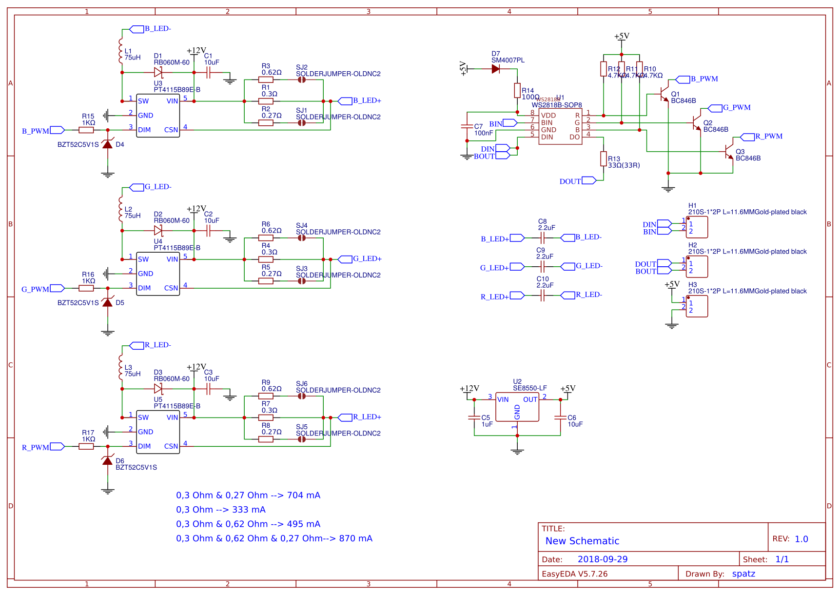
On the left side of the schematic are the three constant current sources based on the PT4115. The inductor has 75µH and 1.15A, which should be in the specified range for the selectable currents. In the datasheet of the PT4115 it says that the rated current should be 30% to 50% higher than the output current. At 870 mA, it is still a little bit above the specifed 30% buffer, at all other currents it is well above the 50% buffer.
The diode is a RB060M-60, as it has low reverse current and is rated at 2A.
The capacitor is a 10µF/25V ceramic, and an additional wired 100µF/25V electrolytic for each IC, which is not in the schematic, as it is directly soldered to the board.
The DIM pin of the PT4115 seems to be rather sensitive to over-voltage and ESD, so it is protected by an additional resistor and Z-diode.
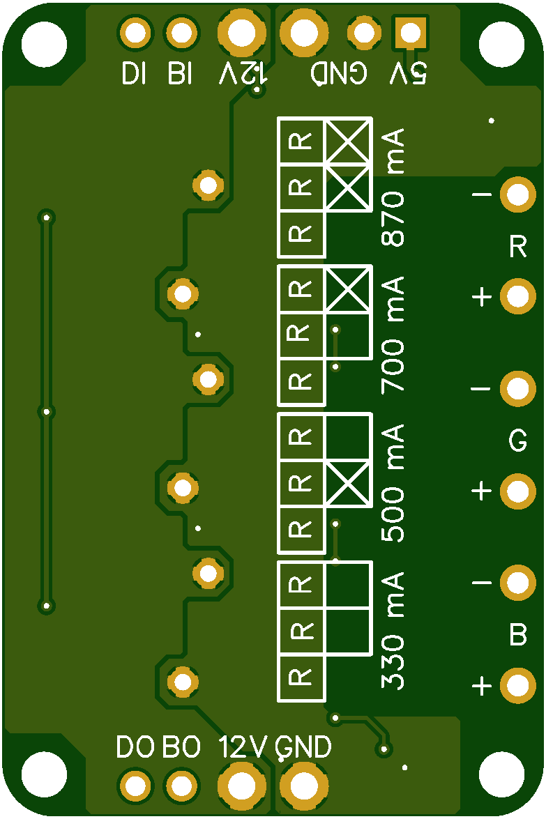
The three current sense resistors have certain values, so that if you connect them in parallel with the solder jumpers, the specified currents are selected. these currents are 330mA, 500mA, 700mA and 870mA. The 0.3Ohm resistor is always connected.
On the right side of the schematic, there's the WS2818, basically a WS2811 with backup input.
The diode on the voltage supply of the WS2818 has a voltage drop of 0,7 Volts. This makes it possible to run the WS2818 directly with a 3.3V input (like the ESP8266). This trick is taken from Hackaday. What I'm wondering: Is it still okay to have an input signal with a voltage of 5V. On one hand, it says the maximum voltage on the input pin is VDD+0.5V, and 5V pinut would be VDD+0.7V, on the other hand the WS2818 is specified for 5V pinut. So, can I mount the diode on every board, or should I put a solder jumper in parallel, in case you're having an 5V input (Arduino etc.)?
The PT4115 expects an active high signal on its DIM pin, whereas the WS2818 gives an active low output. For inverting and level shifting the signal, I took the circuit from the PixiFlood project.
The rest of the parts around the WS2818 are the parts recommended in its datasheet.
The three capacitors (2,2µF/25V) in parallel to the LEDs are there to reduce the ripple current, as recommended in the datasheet of the PT4115. I think this makes sense, as there may be a lot of boards on the same voltage supply, with rather long wires between them.
The LDO for the WS2818 is a Seaward SE8550, as it is small (SOT-23), cheap (4 Cents), takes input voltages up to 35V and delivers 250mA, which should be enough for WS2818 and ESP8266.
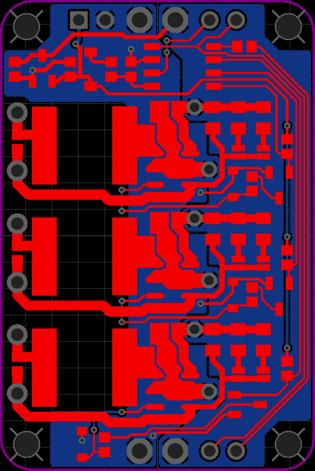
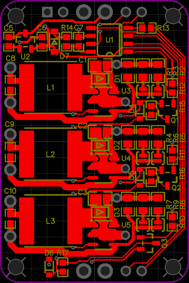
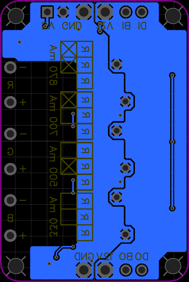
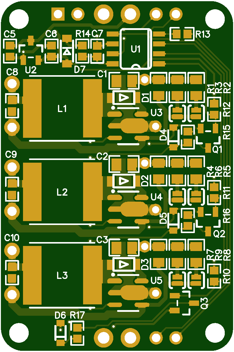
Next comes the PCB, about which I'd like to know wether it's okay like this. I tried to get all parts on 30mm x 45mm, so I can order 60 boards with panelizing via JLCPCBs special offer (2*3*10). I'm especially wondering about the current sense loop and if it's okay to share one part of it with the power supply loop, or if I should have individual traces?
The pads of the electrolytic caps are also the connections between the power supply rails of the back of the board and the LED drivers. The power supply rails on the back are as wide as possible. The connections on the SW, 12V and GND pins of the PT4115 are made with copper fills to be as wide as possible, too. The electrolytic caps are bent to 90 degrees and are mounted above the coils.
The LEDs themselves are mounted via cables, so you can easily mount them to a heatsink.
The DIM pin protection parts of the lowest PT4115 have a slightly different position. Otherwise they might collide with the mounting screws.
Will this layout work?

