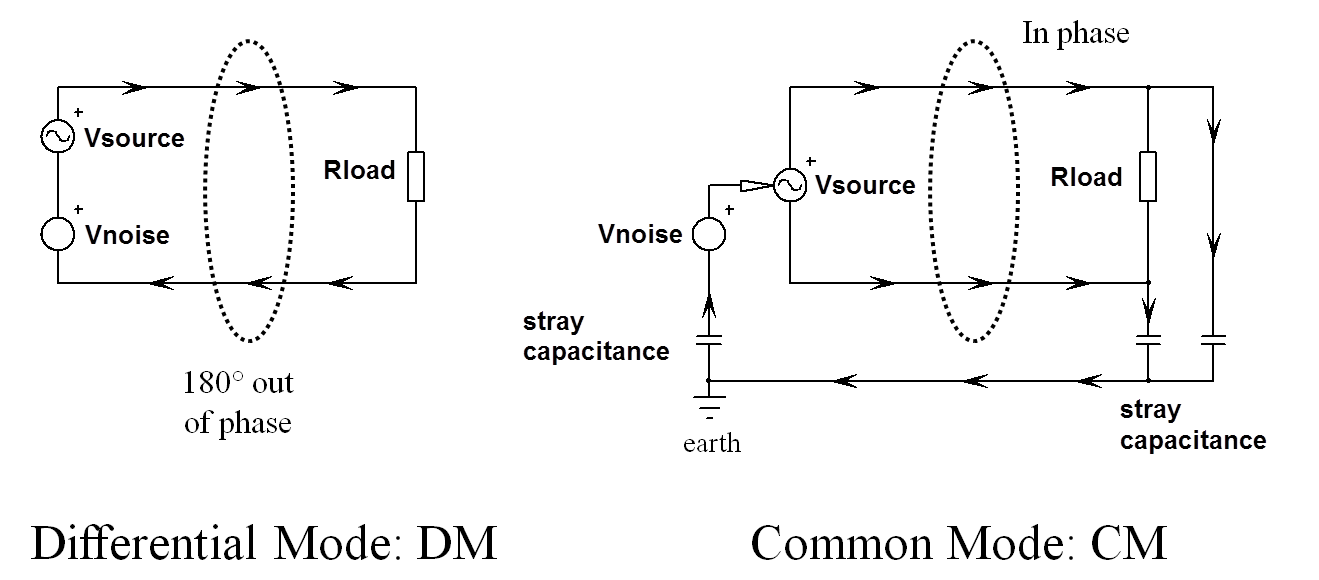
The simple drawing below illustrates the difference between the differential- (DM) and common-mode (CM) conducted perturbation:

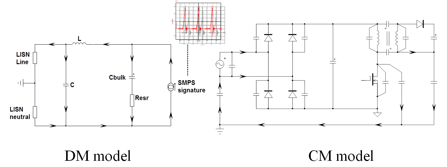
Usually, but it is not always the case, a DM perturbation appears in the low-frequency portion in an EMI plot while CM noise is located in higher frequencies. If you go deeper in the analysis of a switching converter such as a flyback converter, you can imagine the below mechanisms pertaining to conducted perturbations:

In DM, it is the circulation of the high-frequency primary-side current signature in the bulk capacitor which generates the perturbation. The harmonic content depends obviously on the operating conditions and, in particular, in the operating mode, discontinuous (DCM) or continuous (CCM). You fight these perturbations with a differential-mode filter, usually built around the leakage inductance of the common-mode component.
In CM, the coupling mechanism is mainly linked to high dV/dt switching nodes and fast switching components: the stray capacitance between the MOSFET tab and the heatsink, the inter-winding capacitance of the transformer, the rectifying diode and so on. All these parasitics go across isolation barriers via stray capacitances that must be minimized during PCB layout and component construction (transformer). Switching noise on the output is inherently due to the switching nature of the rectified waveform. On top of that, you add the recovery effect of the output diode in CCM which pollutes conducted but also radiated signatures. Minimizing loops area in which high currents circulate and damping all these oscillations are key to solving EMI issues.
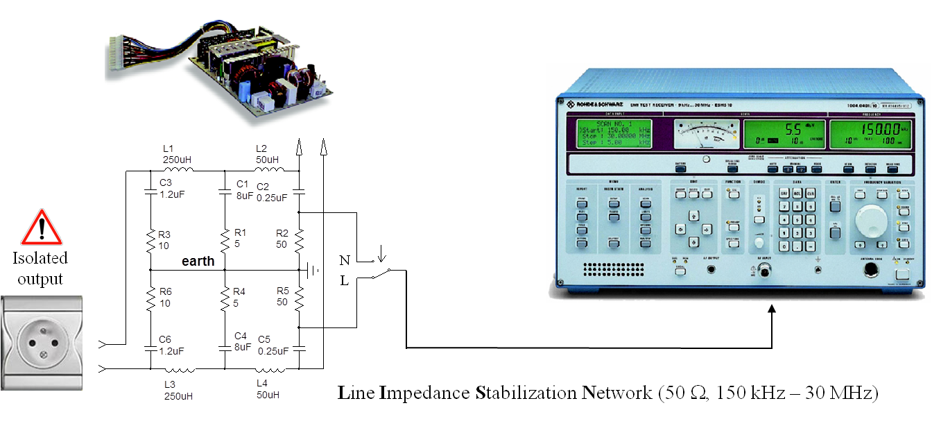
Finally, you measure all these conducted perturbation with a line impedance stabilization network or LISN configured in such a way that you can isolate DM and CM noises. You have to separate CM and DM as each requires a different cure. The LISN offers a constant 50-\$\Omega\$ output resistance along the analyzed frequency band. The final EMI plot to check PASS or FAIL mixes them of course.
