3
\$\begingroup\$

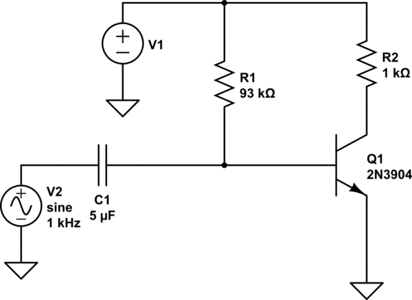
I'm having some trouble understanding the behaviour of the basic common emitter fixed bias amplifier. I've been looking at this for awhile now and I'm starting to think there is a foundational problem with my understanding.

I understand that I need at least 0.7V applied to the base to turn on the base emitter junction, and also that I want to choose R1 so the base current biases the transistor in the middle of it's load line.

My confusion starts when I inject a signal to be amplified. The signal will be superimposed on the bias, however wouldn't that super imposed signal now be varying slightly above and below 0.7V thus turning the transistor off and on, creating a very distorted output signal?

I've tried to think this through and I suspect the current in R1 must start to vary slightly in relation to the input signal?

Another possibility is that I know the base emitter junction doesn't exactly turn off at 0.7V but it does become nonlinear. Would that mean the outputted signal is distored on the negative part of the input signal?

Is this correct?

schematic

simulate this circuit – Schematic created using CircuitLab

\$\endgroup\$
3
  • \$\begingroup\$ Welcome to EE.SE. I've taken the liberty of turning your voltage source the right way up (positive on top) and making the ground symbol point to, um, ground. I also deleted the 1 V parameter on V1 as I reckoned you weren't trying to run the circuit at the default value of 1 V. \$\endgroup\$
    – Transistor
    Commented Feb 19, 2019 at 19:06
  • \$\begingroup\$ Try simulating it. Superposition means you can add up the contributions of each source seperately, while other sources are zero. So, check what V1 does by shorting V2 (setting it to zero volts), next, check the contributions of V2 by shorting V1. \$\endgroup\$
    – Huisman
    Commented Feb 19, 2019 at 19:24
  • 1
    \$\begingroup\$ We never, ever design a transistor bias circuit like that, because the hFE (beta), temperature and supply voltage of the transistor determine the output voltage. If the transistor bias voltage is proper so that there is no clipping then usually the top of the output waveform us squashed with distortion when there is no negative feedback. \$\endgroup\$
    – Audioguru
    Commented Jul 24, 2022 at 0:52

4 Answers 4

3
\$\begingroup\$

Start by taking a look at what happens to collector voltage as base potential varies. We'll also need to see what's happening to base current as base voltage changes. To do this, I've modified your circuit a little to impose a potential directly at the base, and run a DC sweep simulation:
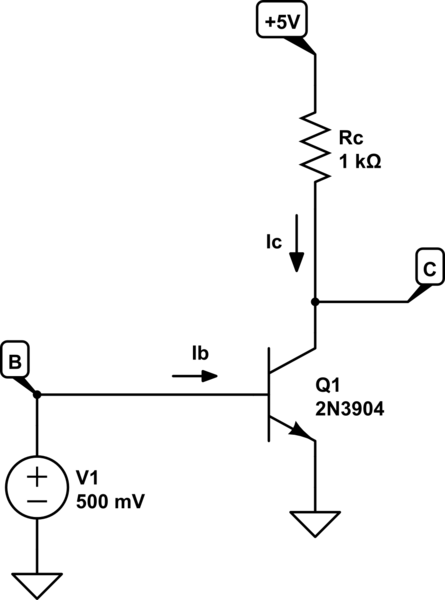
schematic

simulate this circuit – Schematic created using CircuitLab

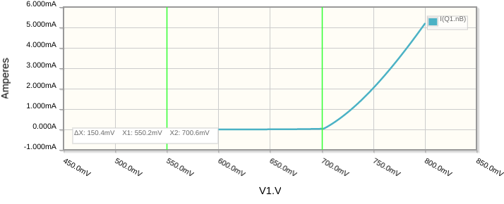
Here are plots of collector voltage and base current:
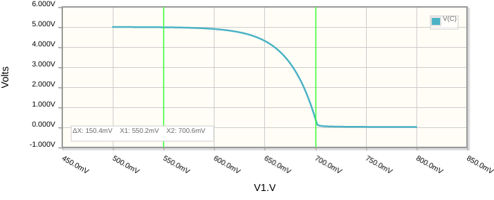
enter image description here enter image description here

The main points of interest on these graphs (marked in green) are:

  • where the transistor begins to conduct from collector to emitter. This happens at a base potential of about 550mV for this model.

  • where the transistor saturates, which is when it can't conduct any better, its effective collector-to-emitter resistance is lowest (close to 0Ω) and the voltage between collector and emitter is as close to 0V as it will ever be. That's at about 700mV here.

Contrary to what a lot of people say on the web, about bipolar transistors being current amplifiers, and not voltage amplifiers, that's clearly not the case here. You can see that a very small change in base potential, from 550mV to 700mV, results in a much larger change at the collector, from 5V to 0V. This is definitely a voltage amplifier, with significant gain.

Notice that base current is small prior to saturation, and rises sharply thereafter. In a linear amplifier, we mostly don't want the transistor to saturate, and we try to avoid this region to the right. To address your question, we must focus on the region between the two markers, where the transistor is operating in a state between cut-off and saturation.

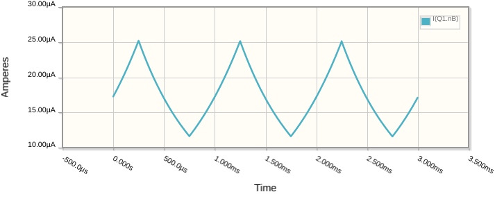
To that end, I want a better idea of base current in this "linear" region (it's clearly not linear, so maybe "active" region would be a better term), since all the above graph tells me is that base current is really small. Zooming in to the active region:
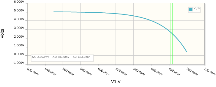
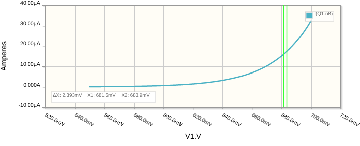
enter image description here enter image description here

Now we have a better idea of base current behaviour in the active region. To bias this transistor, generally the goal is to place it in a condition where its collector voltage is half way between its maximum (here that's +5V) and minimum (0V) values, which would be 2.5V, so that it has as much room above it (prior to cut-off) as it has below (prior to saturation). Looking at the plot of base current vs. base potential, I see that this particular model of transistor, with this particular collector resistor, I require about 17μA of base current, and this occurs when the base is at about 0.68V.

We insert a resistor between base and +5V, that will pass 17μA into the base, from the supply voltage source:
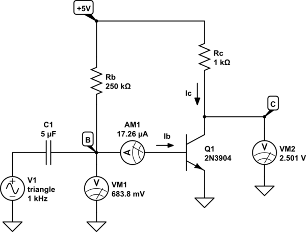
schematic

simulate this circuit

The value I chose for Rb isn't arbitrary. It's calculated using Ohm's law. I know the voltage across it will be the difference between the +5V supply and the base at 0.68V, and we know the current, which is \$I_B = 17\mu A\$.

$$ R_B = \frac{V_{R_B}}{I_B} = \frac{5.0 - 0.68}{17\times 10^{-6}} \approx 250k\Omega $$

The simulation shows us that our collector does indeed settle at 2.5V, and the base current and potential are what we expected.

We are ready to examine the behaviour of the collector, when the base is stimulated by some AC voltage source. First it is necessary to understand the role of capacitor C1. The voltage source V1 will have some average value, and if we connected it directly to the base, it would upset the delicate equilibrium we have established.

The base wants to have an average voltage of 680mV, and V1 wants to centre itself around some other value, say 2V. Capacitor C1 will, over time, charge up to a DC potential difference equal to the difference of those two averages \$V_{C1} = 2.00 - 0.68V \approx 1.3V \$. After that has been achieved, any voltage changes occuring on one side (either side) of C1 will also appear on the other side, shifted up or down by 1.3V. In this way, any DC component of the voltage source V1 is offset by the voltage across C1, allowing the base to maintain its own idea of what "centre" means, without requiring whatever is on the other side to have that same particular DC "centre" too. AC components ("changes" in potential) of V1 are still copied over to the other side. This is the reason why C1 is called an "AC coupling capacitor", or a "DC blocking capacitor".

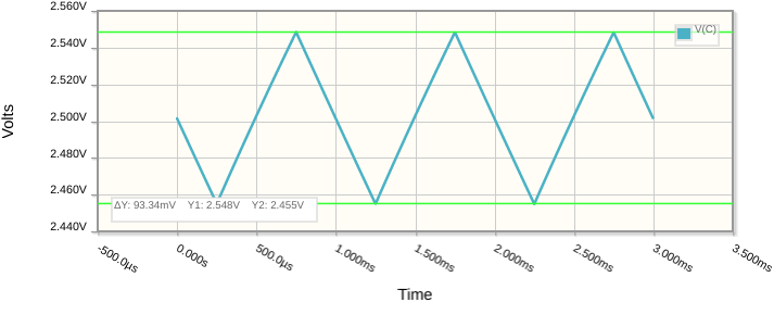
Let's start with a really small input signal, say 0.5mV amplitude (1mV peak to peak). I'll make it triangular, so that we can spot any non-linearity at the output. Here are plots of the input (base potential) and output (collector potential) over time:
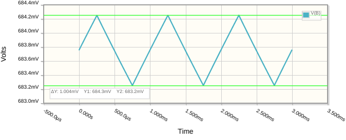
enter image description here enter image description here

The output is a good (inverted) copy of the input, with amplitude 47mV (94mV peak to peak). That's a gain of 94. The reason it seems to have very little distortion is that the region in which the transistor is operating here is a very small slice of the entire active region, between base potentials of 680±0.5mV.

In that region, the graph of base vs. collector potentials (see the very first graph in this answer) approximates a straight line. A small segment of any graph of a continuous function looks like a straight line, if you zoom in far enough. This is an underlying principle of calculus, in which we state that as we examine the behaviour of a function between two points which are infinitesimally close together on the curve, the curve is, for all intents and purposes, a straight line.

This is also the thinking behind the concept of small-signal AC analysis. As we'll see in a moment, if the signals you use to model the behaviour of a system are too large in amplitude, you end up driving the system into non-linear regions. By keeping all input signals tiny, and the corresponding output signals are also tiny, all the curves of all the functions describing the system become straight lines, and the system can be treated as "linear", which has many benefits both from a complexity perspective, and a mathematical perspective.

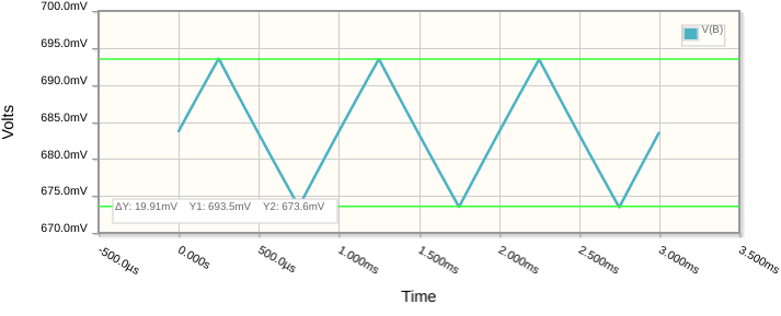
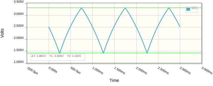
Let's over-drive the input, so that we use a wider chunk of the active region, without entering cut-off or saturation. This should illustrate the points about linearity I made above, and finally answer your question. With an input of 10mV amplitude (20mV peak to peak), base and collector voltages look like this:
enter image description here enter image description here

As you can see, the output is no longer a very good copy of the input, and a lot of distortion is apparent. We are employing a region of base potential between 673mV and 693mV, a much wider range. If you look at the first graph in this answer, you can see clearly that the line (of collector voltage) between 673mV at the base and 693mV, is very curved, and that's why the output is so distorted.

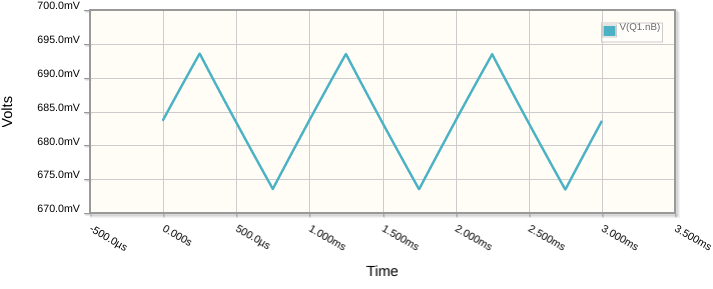
Finally, to touch on your idea that base current must vary slightly too, you are correct. Base current will fluctuate as base voltage fluctuates, because those people who claim that a bipolar junction transistor is a current amplifier are in fact right. It's the ones who claim that it's not a voltage amplifier who are wrong.

Let's take a look at base current corresponding to the 20mV base signal we applied last:
enter image description here enter image description here

So yes, the base current does fluctuate in response to applied base potential, and in this sense the amplifier is operating both as a current amplifier and a voltage amplifier, depending on your perspective.
\$\endgroup\$
1
\$\begingroup\$

The transistor does not just go from hard on to hard off. Rather, the emitter current of the transistor follows the diode equation. Roughly, \$i_e = I_{SS}\left(e^\frac{v_{be}}{V_T} - 1\right)\$ (Google for the diode equation for the definitions of \$I_{SS}\$ and \$V_T\$). At room temperature, \$V_T \simeq 26\mathrm{mV}\$.

So in your simple circuit, a small (like, less than 1mV or so peak-peak) signal will act to increase and decrease the emitter current in an amount proportional to the signal voltage.

\$\endgroup\$
2
  • \$\begingroup\$ I think I may have thought of a better way of asking my question. In the basic circuit I've drawn, would the output signal be distorted on the negative peak of the input signal? When I look at the graph of the diode equation, I believe the answer is yes. \$\endgroup\$
    – lowteq
    Commented Feb 19, 2019 at 21:55
  • \$\begingroup\$ It depends on how small your input signal is. The percentage distortion will get arbitrarily small as you reduced the input signal amplitude. \$\endgroup\$
    – TimWescott
    Commented Feb 19, 2019 at 21:57
1
\$\begingroup\$

I understand that I need at least 0.7V applied to the base to turn on the base emitter junction,

Not exactly. A base-emitter junction can be considered forward-biased with larger or smaller magnitudes than \$700\:\text{mV}\$. It's just that the collector current (speaking now about common small-signal BJTs) will change by roughly a factor of 10 for every \$60\:\text{mV}\$ change in the base-emitter voltage. So if \$I_\text{C}=1\:\text{mA}\$ when \$V_\text{BE}=670\:\text{mV}\$, then you might expect that \$I_\text{C}=100\:\mu\text{A}\$ when \$V_\text{BE}=610\:\text{mV}\$ (assuming the temperature didn't change and you are using the same BJT as before.)

and also that I want to choose R1 so the base current biases the transistor in the middle of it's load line.

Again, that depends. But yes, you want to bias the BJT somewhere useful. How you make that decision may involve a little more than just "middle of...."

My confusion starts when I inject a signal to be amplified. The signal will be superimposed on the bias, however wouldn't that super imposed signal now be varying slightly above and below 0.7V thus turning the transistor off and on, creating a very distorted output signal?

Actually, for your circuit it's quite true that the output signal will be distorted. It's one of the reasons that it's not used (much) without some kind of global NFB included. You are looking at a grounded emitter, so the only AC impedance will be \$r_e=\frac{V_T}{I_\text{C}}\$, where \$V_T\$ is the thermal voltage.

To a first order approximation, \$I_\text{C}\$ follows the Shockley equation. And that means that approximately a 10-fold change in \$I_\text{C}\$ for a \$60\:\text{mV}\$ change in \$V_\text{BE}\$. So once again, suppose \$I_\text{C}=1\:\text{mA}\$ and that you've biased things so that \$V_\text{BE}=670\:\text{mV}\$. From this, the voltage gain will be hovering at about \$A_V=\frac{R_\text{C}=1\:\text{k}\Omega}{r_e\approx 26\:\Omega}\approx 38.5\$. Suppose your AC signal is \$v_{ac}=\pm25\:\text{mV}\$. Near the top of the positive-going swing, it pulls upward on the base by \$25\:\text{mV}\$ and this causes the collector current to increase by a factor of about 2.6. So the gain raises to about \$A_V=\frac{R_\text{C}=1\:\text{k}\Omega}{r_e\approx 10\:\Omega}\approx 100\$. Near the bottom of the negative-going swing, it pulls downward on the base by \$25\:\text{mV}\$ and this causes the collector current to decrease by a factor of about 2.6. So the gain falls to about \$A_V=\frac{R_\text{C}=1\:\text{k}\Omega}{r_e\approx 68\:\Omega}\approx 14.8\$. In short, the voltage gain is varying with the signal, everywhere from about 15 to about 100.

So yes, the signal at the collector is usually distorted. If you keep the input signal swing small enough, say below a millivolt or so, then it's not so bad. But this kind of stage isn't often used as a single stage. Instead, global NFB as part of a multi-stage system is often applied to help straighten things out. (Or an emitter resistor is added to provide local NFB.)


So far, I've just addressed your questions. But the circuit isn't very good. Different BJTs from the same family of parts will vary significantly in a variety of ways. They will have different saturation currents which affect their base-emitter voltage for a given collector current; they will exhibit different values of \$\beta\$; they will vary somewhat differently as the ambient temperature rises and falls during the day; etc. If you do know how to calculate (in theory) the operating point given some varying parameters, try it out and see how differently that circuit biases itself with slight variations in these three parameters. If not, use Spice and see what it says. Most especially, play around with \$\beta\$ and see what happens. (Assuming you can get it into active mode and not saturated, of course.)

\$\endgroup\$
1
\$\begingroup\$

When you are superimposing the signal on top of the bias voltage, you have to make sure that the signal is "well-behaved". You cannot expect the circuit to work for all kinds of possible inputs. The definition of "well-behaved" depends on what you are trying to do with the circuit. Since in the question you are trying to make a linear amplifier, you have to assume that the signal follows the small-signal discipline/approximation and it needs to be ensured that the BJT is in forward-active region.
For that, as you said, the \$V_{BE}\$ needs to higher than 0.6V or 0.7V (This is also an approximation) and the \$V_{CE}\$ needs to be higher than ~0.2V. If you assume that 1mA current flows through the collector, then the collector voltage becomes 4V (assuming 5V supply). In this case you have maximum output swing of \$min(1V,3.8V) = 1V\$. Since small signal gain comes around 40, the allowed input swing becomes 25mV (=1/40).
But remember that this gain is derived using small signal approximation. So indeed as you said, in reality you will have some distortion. In this particular case, since, $$I_c = I_se^\frac{V_{be}}{V_t}$$ $$I_C+i_c = I_se^\frac{V_{BE}+v_{be}}{V_t} = I_Ce^\frac{v_{be}}{V_t}$$ $$I_C +i_c = I_C(1+\frac{v_{be}}{V_t}+\frac{1}{2}(\frac{v_{be}}{V_t})^2+...)$$ $$i_c = \frac{I_C}{V_t}v_{be}+ \frac{I_C}{2}(\frac{v_{be}}{V_t})^2...$$ Here the capital letters refer to the bias voltages and the small letters refer to the variations. Clearly, the first term is what you get from the small signal approximation, where you assume that the higher order terms do not matter as they are very small.
In reality, you will get some distortion due to these higher order terms and to ensure that your amplifier is sufficiently linear, you would need to ensure that \$\frac{V_t}{v_{be}}\$ (ratio of the first two terms called harmonic distortion) is high accordingly. So for higher linearity, you need to reduce your input swing.

\$\endgroup\$

Your Answer

By clicking “Post Your Answer”, you agree to our terms of service and acknowledge you have read our privacy policy.

Not the answer you're looking for? Browse other questions tagged or ask your own question.