1
\$\begingroup\$

diagram

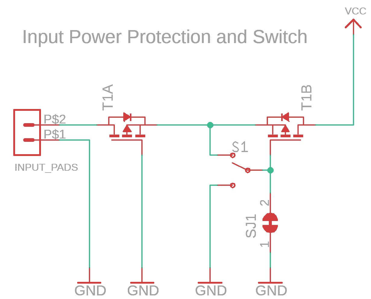
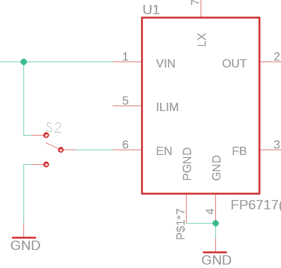
I'm designing a simple board with a FitiPower FP6717 step-up converter chip (Datasheet) and a mechanical switch (SPDT) to enable or disable the output power. My design for the boost will be very close to the typical application circuit in the datasheet. What is the best practice in terms of switch location? Here are the two options I've narrowed it down to:

  1. Enable/disable the input power from a battery with a PFET at the input with the switch (VCC goes to the Vin pin of the FP6717):

Input

  1. Enable/disable the input power by switching the EN pin on the FP6717 between GND and Vin:

EN

Is there a "correct" answer to this? My gut tells me to put it on the EN pin, since there will be some non-zero power dissipated over the PFETs RDS(ON), which would decrease the overall efficiency from the battery to the output.

\$\endgroup\$
1
  • 2
    \$\begingroup\$ Depending on how often you want to switch it on/off, why not insert the mechanical switch directly between the battery and Boost converter? You didn't state your input and output requirements, but Vin,max = 5.25V or about Iin,max = 6Adc max (with 3A load at 3Vin) are not that high to switch mechanically. \$\endgroup\$
    – Huisman
    Commented May 16, 2019 at 11:04

1 Answer 1

1
\$\begingroup\$

There is no general answer for this. You will have to check the datasheets of the components for both solutions and pick the one that has lowest battery drain.

\$\endgroup\$

Your Answer

By clicking “Post Your Answer”, you agree to our terms of service and acknowledge you have read our privacy policy.

Not the answer you're looking for? Browse other questions tagged or ask your own question.