3
\$\begingroup\$

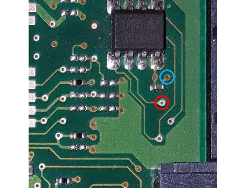
Here's an area of a commercial PCB.

I'd like to know if the "missing" solder mask is a deliberate choice made by the PCB designer, and if so, why?

edit: changed graphic to highlight representative vias.
Blue circle - solder mask (gold-colored)
Red circle - no mask (silver colored)


enter image description here

\$\endgroup\$
1
  • 1
    \$\begingroup\$ Test points is my guess. Perhaps there's no where else you can probe that particular test point except on the top (or bottom) layer. The ODM's and the engineers that developed this would be the only ones to know where exactly everything is wired. \$\endgroup\$
    – user103380
    Commented May 16, 2019 at 20:32

3 Answers 3

4
\$\begingroup\$

It's an option in most PCB design software, both as a default and on a per-via basis.

The advantage of leaving the vias uncovered is you can probe them with test probes without having to scrape away the solder-mask first. The advantage of covering them is reduced risk of shorts or solder-stealing.

Personally I tend to start with them uncovered, but then cover the ones close to components.

I wonder if in your case the designer has made them covered by default on the power/ground nets, but uncovered by default on signal nets. That could make some sense as power/ground vias are less likely to need to be probed and are more likely to be in tight locations.

\$\endgroup\$
1
  • 1
    \$\begingroup\$ At first it seemed unlikely to me that the board would need as many TPs as there were unmasked vias, but after carefully looking over the board I can see that there is only one unmasked via per node so that gives credibility to that being the reason. \$\endgroup\$
    – mike65535
    Commented May 20, 2019 at 13:21
2
\$\begingroup\$

Yes, it's a choice in most PCB design software.

It might be a default choice or it might be a deliberate choice, you'd have to ask the designer.

Sometimes vias double as test points (in which case they are specified without solder mask), but at first glance, I don't see evidence of that in the sample. The board appears to be Organic Solderability Preservative (OSP) finish, which would not be great for test points. ORP is used in high volume consumer electronics because it's cheap (no gold).

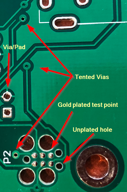
Here is a PCB with ENIG (electroless gold over nickel barrier) finish that has both kinds of vias/pads. As you can see, the tenting is not always perfect sometimes it pulls away around the edges of the holes.
enter image description here

\$\endgroup\$
6
  • 1
    \$\begingroup\$ Yes, but why choose to mask some holes, and not others? I thought perhaps for test points, but does a 5cm x 9cm board need ~200 tp? \$\endgroup\$
    – mike65535
    Commented May 16, 2019 at 20:24
  • \$\begingroup\$ Which ones do you think are masked? I don't see any tented ones at all, so it looks like a global choice, default or deliberate. \$\endgroup\$ Commented May 16, 2019 at 20:26
  • \$\begingroup\$ It appears to me that the gold-colored vias are masked, while the silver-colored ones are not. \$\endgroup\$
    – mike65535
    Commented May 16, 2019 at 20:36
  • \$\begingroup\$ It looks like it's got some kind of plating (tin perhaps) for an edge connector that's at the left edge of your photo. I don't think it's deliberate whether it got on some vias & not on others, maybe just a processing artifact. I don't see any gold at all, just ORP copper and plating. \$\endgroup\$ Commented May 16, 2019 at 20:39
  • \$\begingroup\$ I updated the post \$\endgroup\$
    – mike65535
    Commented May 16, 2019 at 20:50
1
\$\begingroup\$

I'd like to know if the "missing" solder mask is a deliberate choice made by the PCB designer, and if so, why?

The main reason would probably to have something to solder to or test points. I have all of my vias made with the solder mask removed, and unless there are size limitation from needing lots of vias in a small space, I make them the size of 34 gauge blue wire. This makes it easy to solder in wires for test monitoring equipment, like an oscilloscope. If I have soldermask on the via, I have to remove it with an exacto knife. Vias also make great points to stick digital multi meter probes in (if they have no solder mask)

\$\endgroup\$

Your Answer

By clicking “Post Your Answer”, you agree to our terms of service and acknowledge you have read our privacy policy.

Not the answer you're looking for? Browse other questions tagged or ask your own question.