2
\$\begingroup\$

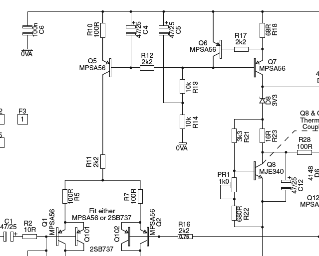
I'm reading Douglas Self's Audio Amplifier Design, and there is a circuit presented with a current source I can't understand.

enter image description here

The source would be the one formed by Q5, Q6 and Q7. If Q6 would be 'flipped', with its emitter on the base of Q7 and its base on the colector of Q7, I would recognize it as a bipolar mirror with base-current compensation, but I can't understand how this one works.

\$\endgroup\$
1
  • \$\begingroup\$ Q6+ R17 just offers a soft current limit to regulate driving the next final stage, since the DC negative feedback loop gain is low, ~< (R13+14)/R17) = 10 \$\endgroup\$
    – D.A.S.
    Commented Jun 4, 2019 at 14:03

5 Answers 5

5
\$\begingroup\$

I gather you are talking about Figure 12.12 from the 5th edition. Here's the schematic redrawn, just slightly:
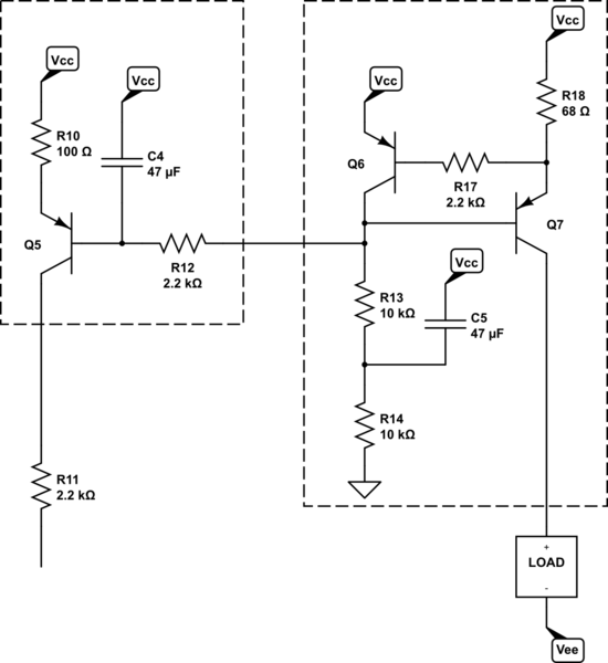
schematic

simulate this circuit – Schematic created using CircuitLab

You can see a very similar circuit to the portion of the above circuit within the right box in an answer I provided here. Note that I didn't include the equivalent of \$R_{17}\$ in that circuit (it's not strictly needed.) And note that it is based on NPN BJTs, instead. But the concept is about the same.

Resistors \$R_{13}\$ and \$R_{14}\$ turn on \$Q_7\$ and \$Q_6\$ by providing a current sink of about \$I_{R_{14}}=\frac{V_\text{CC}-2\cdot V_\text{BE}}{10\:\text{k}\Omega+10\:\text{k}\Omega}\$. Assuming \$V_\text{CC}\$ is on the order of about \$45\:\text{V}\pm 5\:\text{V}\$ this is on the order of around \$2\:\text{mA}\$.

The actual value of \$I_{R_{14}}\$ isn't that important, because the excess is handled by \$Q_6\$. The rest provides the needed base recombination current for \$Q_7\$, whose base-emitter junction is certainly now forward-biased.

\$Q_6\$'s base is pulled down by the emitter of \$Q_7\$, turning \$Q_6\$ on, as well. So both BJTs are definitely active. Ignoring \$R_{17}\$ for now, \$Q_6\$'s \$V_\text{BE}\$ "sets" the voltage across \$R_{18}\$, which will be one base-emitter drop.

So, assuming \$V_{\text{BE}_{Q_6}}=700\:\text{mV}\$, then \$I_{R_{18}}=\frac{V_{\text{BE}_{Q_6}}}{68\:\text{k}\Omega}\approx 10.3\:\text{mA}\$ and that also sets the collector current of \$Q_7\$.

Given that collector current, it is likely that \$V_{\text{BE}_{Q_7}}\ge 700\:\text{mV}\$ and that the base recombination current of \$Q_7\$ will be on the order of 100 times smaller (or still less), or about \$I_{\text{B}_{Q_7}}\approx 100\:\mu\text{A}\$. We already calculated \$I_{R_{14}}\approx 2\:\text{mA}\$, which is therefore far more than enough for \$Q_7\$'s base. The rest is disposed of by \$Q_6\$'s collector. So we can expect that \$Q_6\$'s collector current is also close to \$2\:\text{mA}\$ and that confirms the previous assumption that \$V_{\text{BE}_{Q_6}}=700\:\text{mV}\$. Q.E.D.

So the "LOAD" on the right is seeing a constant current source of about \$10\:\text{mA}\$ as a result of the circuit on the right.

(The base recombination current of \$Q_6\$ will be \$I_{\text{B}_{Q_6}}\le 20\:\mu\text{A}\$. \$R_{17}\$ is there to help protect \$Q_6\$ should the load wind up short-circuited.)

Moving over to the left side, now.

\$Q_7\$'s base voltage is pretty stable and will be approximately two \$V_\text{BE}\$ voltages below \$V_\text{CC}\$. (\$Q_6\$'s plus \$Q_7\$'s plus a tiny drop for \$R_{17}\$.) I expect it to be about \$1.5\:\text{V}\$ below \$V_\text{CC}\$. This \$Q_7\$ base voltage is then presented to the base of \$Q_5\$ via \$R_{12}\$.

Assuming no voltage drop for \$R_{12}\$ for a moment, we'd expect the emitter current of \$Q_5\$ to be about \$I_{\text{E}_{Q_5}}=\frac{1.5\:\text{V}-700\:\text{mV}}{R_{10}=100\:\Omega}\approx 8\:\text{mA}\$. This implies \$I_{\text{B}_{Q_5}}\le 80\:\mu\text{A}\$ and therefore a voltage drop across \$R_{12}\$ of \$180\:\text{mV}\$. This lowers the computed collector current for \$Q_5\$ towards about \$6\:\text{mA}\$. (No point in being overly-precise, though, so these numbers are only approximate.)

(Again, \$R_{12}\$ and \$C_4\$ provides some isolation and base voltage stability as well as some thermal and BJT variation handling.)

So \$Q_5\$ is just another current source. But with a set point that is a little different from \$Q_7\$'s, determined by the different emitter resistors being used by them.

\$Q_6\$ soaks up (via its collector) the excess current supplied via \$R_{13}\$ and \$R_{14}\$ (using \$C_5\$ to seriously stiffen up their current sinking behavior at AC.) This collector current is high, compared to the base current used by \$Q_7\$, so that the variations in \$Q_6\$'s \$V_\text{BE}\$ will only very slightly impact the base voltage that is passed over to \$Q_5\$.

\$\endgroup\$
4
  • \$\begingroup\$ What about the AC voltage response effects of Q6 to overall? \$\endgroup\$
    – D.A.S.
    Commented Jun 4, 2019 at 18:10
  • \$\begingroup\$ What is your thought about R11? And how would you pick a value for R17 \$\endgroup\$
    – G36
    Commented Jun 4, 2019 at 18:47
  • \$\begingroup\$ @G36 \$R_{11}\$ feeds to another part of the circuit I didn't want to talk about (and isn't in the OP's question.) I made a mistake regarding \$R_{17}\$ and I'm glad you asked about it. I was writing on "automatic pilot" (actually, I was doing a lot of tractor work outside today) and thinking about the base resistor that is added to a current mirror for the reasons I mentioned. But in this case, there's a different reason. So I'm changing the text to correct my mistake there. Thanks! \$\endgroup\$
    – jonk
    Commented Jun 5, 2019 at 2:53
  • \$\begingroup\$ Really great answer! Thanks a lot! \$\endgroup\$
    – MPA95
    Commented Jun 5, 2019 at 13:07
3
\$\begingroup\$

I agree with all the answers so far but would like to add a different perspective.

The purpose of Q6 as a Q7 current limiter is to make the AC impedance of Q7 so high that it does not introduce any significant AC nonlinearity. This permits the next 4(?) stages of NPN/PNP Emitter Followers to buffer the AC load impedance scaled by each hFE.

This results in very high Voltage massive† AC open loop voltage gain followed by very high current gain. The output is then fed back to an R divider thru R16 to regulate the closed loop gain.

The DC tolerance and stability of the DC current is not critical thru Q7 but since Ib of Q6 < 100uA the voltage, it's Vbe will be well under 0.6V but V(R18) closer to 0.6V and thus 0.6V/68Ω = 8.8mA but this could easily be +/- 25% with temp and tolerances and not affect the AC loop current gain of Q6*Q7 that regulates the constant AC current. *This would rise to 10mA with Vcc=45. (soft DC limiter) and Pd(Q8)=24V*10mA= 1/4W*

The DC current is not so constant, and drifts with temperature on Vbe but doesn't matter as much. So I called Q6 a soft current limiter (for DC), but its real purpose is to eliminate AC current load on the hidden collector below Q8-e and thus very high open loop gain, at any desired value of DC current selected by 0.6V/R18.

The advantage of this method is high PSRR and high linearity with no AC current out of Q7-C (other than the Early Effect current (~1 uA) for a Common Emitter (CE) amplifier. It is also insensitive to hFE for Q7/8.

When CE amplifiers are used as voltage amplifiers the AC current on the collector must be held constant to the desired tolerance for THD high quality <0.1%.

The main disadvantage is the Miller capacitance of Q7 limits the GBW of this stage but is OK for Audio BW and is approaching prudent thermal limits of Q7.

Douglas Self uses the term voltage amplifier stage (VAS) otherwise known as a "transadmittance" stage using this current source on the collector.

enter image description here

†( as Mr. Self calls it)

Any comment on R11 and how to select R17 value?

  1. R11 only serves to share dumping P=VI, DC power with Q5. If I ≈ 6mA then R11 dissipates 132 mW and reduces Q5 to some(?) value below 200mW.

  2. R17 controls all the collector current of Q6 from R13+R14 (2 to 2.5mA) and leaves a small amount for both base currents I would choose R17 = 10% of R13+14 which affects CC value as much hFE variations of 300%. It's not critical. So I would pick 2K +/-1K. The high open loop gain is DC stabilized by the negative feedback via R16. The lower R17 value reduces the current mirrors slightly and thus runs Q5 & Q7 a bit cooler.

\$\endgroup\$
3
  • \$\begingroup\$ Any comment on R11 and how to select R17 value? \$\endgroup\$
    – G36
    Commented Jun 4, 2019 at 18:50
  • \$\begingroup\$ Great answer! I see how increasing the AC impedance of the current source would increase the open loop gain (by increasing the load of the VAS stage, I suppose), but I don't understand how Q6 increases the AC impedance of Q7. It would be great if you could give a little explanation on that! \$\endgroup\$
    – MPA95
    Commented Jun 5, 2019 at 13:32
  • \$\begingroup\$ I could but you already accepted an answer. \$\endgroup\$
    – D.A.S.
    Commented Jun 5, 2019 at 14:06
3
\$\begingroup\$

Quite a lot going on in these 3 transistors.

View Q6/R13/R14 as a high-gain common-emitter amplifier; the addition of C5 serves to cut the AC gain in half, but greatly boosts the AC Power Supply Rejection. Common-emitter resistive-load stages have gains of Vdd/0.026 at the most (when Vce is very low, as in this case); assuming 50 volt rails, the gain is 50 * 39 * 0.5(our C5 in action) or 1,000.

Thus Q6/Q7 is 1,000X stiffer, and devices with poor Vearly (bipolar Rout) will still produce a very stiff load resistance for the entire audio amplifier open-loop gain node, which is the collector of Q7.

Now we have Q5/C4/R12. Given a non-zero Cob (collector-base capacitance) of Q7, and the essentially rail-rail swings on collector of Q7, there will be significant dynamic charge coupling thru Q7 Cob --- 10pF * 50 volts at 20KHz produces 5MegaVolt/sec across 10pF or 50 microAmps exiting base of Q7.

We view C4/R12 as low-pass filter that disrupts this feedback path.

Douglas Self has several books on power amplifier design. He discusses the many gotchas he is aware of, and takes the reader thru a series of UPGRADES of the circuits by explaining how the new circuit(s) cures some of the flaws of the prior circuits. Quite educational and well written.

\$\endgroup\$
2
  • \$\begingroup\$ What about R11? How would you select the R17 resistor value? \$\endgroup\$
    – G36
    Commented Jun 4, 2019 at 18:46
  • \$\begingroup\$ Just read snippets of the book and found it consistent with my understanding and humorous as well. \$\endgroup\$
    – D.A.S.
    Commented Jun 4, 2019 at 20:11
1
\$\begingroup\$

A little more than a Q6 VBE across R18 turns Q6 on, which then shunts away the bias coming through R13, R14 to Q7. So Q6 and Q7 servo the voltage across R18 to be roughly constant. The voltage on Q7 base is then its VBE more than this, so after Q5's VBE, the voltage on R10 is the same as that on R18.

I'm happy with Q5 and Q7 VBE's tracking, but R18 voltage hardly looks constant with temperature. I wonder if it's bucking something else out for the biassing of Q101 etc?

I do feel that Mr Self tends to go over the top with current source stability.

\$\endgroup\$
0
\$\begingroup\$

Q6 and Q7 form a constant current source of about 10.3mA at Q7's Collector.

Q5 is simply a relative mirror of 7mA using the Base voltage of Q7 as its reference. Q5 has nothing to do with the Q6/Q7 CC source.

\$\endgroup\$

Your Answer

By clicking “Post Your Answer”, you agree to our terms of service and acknowledge you have read our privacy policy.

Not the answer you're looking for? Browse other questions tagged or ask your own question.