1
\$\begingroup\$

I am reverse-engineering a daughter card which uses a ADV7125KSTZ140 VGA video DAC driven by a FPGA. The FPGA is a Xilinx Spartan 3E programmed by an off-board processor using slave-serial mode, meaning the daughter card does not require any firmware whatsoever. It also means I do not have any access to the code.

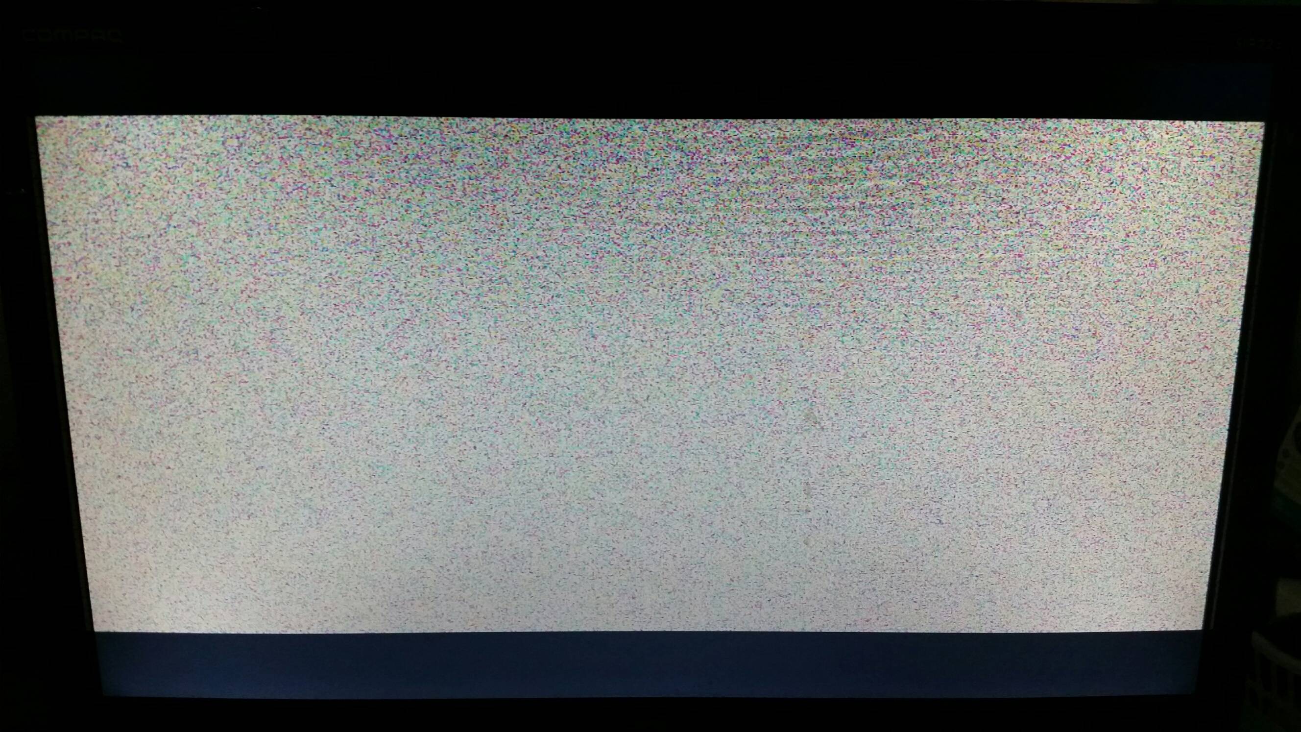
After probing around the board for a couple of weeks, I believe I traced out the entire schematic which can be found in PDF format here. Unfortunately, the board does not work. When plugged into the main device, this is the video output I am getting:

enter image description here

The "static" shown on the screen does not change, it is perfectly still, suggesting it's not simply noise. Unfortunately I have zero experience with VGA, so I am not sure what might cause this - bad data? Bad sync? Missing connections? I am hoping that someone with more experience in this area would be able to check my schematic and see if there are any blatant problems with the design. It is quite possible that I missed some connections during my probing, though all of the connections in the schematic seem logical to me.

If further information is required, please let me know and I will update the question.

UPDATE:

After reading Dave's comments I took another look at the original board again this afternoon. I did some more probing, this time with a meter which had sharper probes. I was able to find several missing/mislabeled connections, which I have now updated. The new schematic can be found here. As I mentioned earlier, my /CE1 was not connected correctly. It should have been connected to /CE3 (mislabeled in the original as /OE3) and also to the MODE and ZZ pins of the SRAM. The connection between /OE and the input of the inverter was correct, but I had left out something very important - the driving source. This should have been connected to Pin 143 of the FPGA, which was originally incorrectly labeled as FPGA_HSWAP.

I do seem to be missing a driving source for the /BW pins though. /BWA, /BWB, and /BWE are all tied together, and pulled high through a 4.53k resistor. I cannot seem to find a connection to the FPGA though, or anything else on the board for that matter. I can't imagine the Byte Write pins can be held high permanently, can they? It seems to me in order to do much of anything with the SRAM you'd have to be able to write to it....

I am wide open to ideas and suggestions of what's going on here.

\$\endgroup\$
8
  • 4
    \$\begingroup\$ If the "static" is unchanging, that means that you're looking at the "random" contents of an uninitialized frame buffer, over and over again. Obviously, the FPGA is getting configured; otherwise, you wouldn't get anything on the screen at all. Presumably software running on the "main device" should be writing to that frame buffer, but that isn't happening. Can you describe that main device in any greater detail? \$\endgroup\$
    – Dave Tweed
    Commented Aug 2, 2019 at 0:39
  • \$\begingroup\$ Sure thing. The main device is an Agilent DSOX3024A oscilloscope. This board is my homebrew version of the DSOXLAN LAN/VGA module. The purpose of the module is not only to provide a LAN interface through an Ethernet connector, but also provide a VGA output to a larger screen, since the scope's screen is rather small. \$\endgroup\$
    – DerStrom8
    Commented Aug 2, 2019 at 0:41
  • \$\begingroup\$ AKA DSOX3000-805, as found here? Do you have a service manual for the scope? That might help explain any connections in the edge connectors that would allow the software to correctly identify your board. \$\endgroup\$
    – Dave Tweed
    Commented Aug 2, 2019 at 0:53
  • 1
    \$\begingroup\$ It's actually perfectly reasonable not to use byte writes in this application, but rather just do /GW (global writes) -- entire 18-bit pixels -- instead. The key would be /SRAM_OE -- does it ever go high? Without any information on the myriad connections between the FGPA and the host system, it's difficult to speculate about how that interface is intended to work. \$\endgroup\$
    – Dave Tweed
    Commented Aug 3, 2019 at 0:33
  • 1
    \$\begingroup\$ Do you have FPGA development tools -- Xilinx ISE, Chipscope, JTAG interface, etc.? It would be relatively straightforward to turn the FPGA itself into a logic analyzer to assist with reverse-engineering the host interface. \$\endgroup\$
    – Dave Tweed
    Commented Aug 3, 2019 at 1:04

1 Answer 1

1
\$\begingroup\$

Short answer:

The SRAM "chip enable" (/CE) and "output enable" (/OE) pins were not properly driven, and that caused the error seen in the original post.

Long answer:

After some back-and-forth in the comments with Dave Tweed, it was determined that the SRAM, which acts as the VGA frame buffer, was not being properly initialized. The video output from the DAC was simply uninitialized information that existed in the SRAM. Otherwise the FPGA and video DAC seemed to be operating correctly, allowing us to narrow down the issue to the SRAM.

After a brief review of the SRAM connections in the schematic, we found a few mistakes and missing connections:

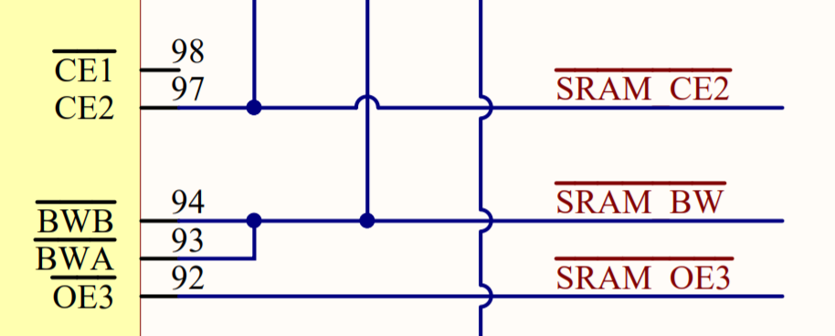
  • There was no connection to /CE1 (chip enable 1). Therefore, the chip was not being properly enabled.
  • /CE3 (chip enable 3) was improperly labeled as /OE3, and not connected to /CE1

enter image description here

  • The output enable pin of the SRAM, /OE, had no driving source. It was only connected to the input of the NC7S04 inverter.

enter image description here

The solutions were simple:

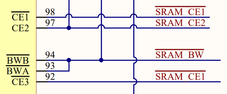
  • Connect /CE3 to /CE1

enter image description here

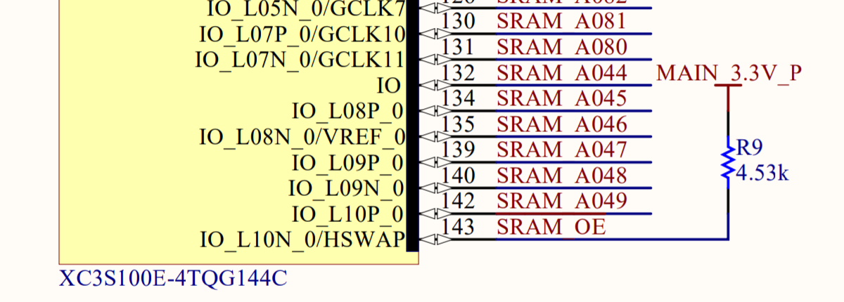
  • Add the missing connection between /OE and the FPGA (discovered to be Pin #143, "IO_L10N_0/HSWAP"), which has a 4.53k pullup to 3.3V

enter image description here

I also discovered that the ZZ (sleep enable) pin of the SRAM on the original board was tied to the MODE pin, which was pulled to ground through a 4.53k resistor. This was not as crucial, though, because the chip already has an internal pull-down for the ZZ pin. Nonetheless, I marked it as a required change.

I made the modifications by soldering some #34 AWG enameled wire to the appropriate pins on the clone board and plugged it into my scope. Sure enough, everything worked as expected. I guess only 2-3 missing connections on a reverse-engineered 6-layer board that was completed without damaging the original is pretty good, all things considered!

\$\endgroup\$

Your Answer

By clicking “Post Your Answer”, you agree to our terms of service and acknowledge you have read our privacy policy.

Not the answer you're looking for? Browse other questions tagged or ask your own question.