Yes, use flux, I've hand soldered QFP's with a soldering iron before.
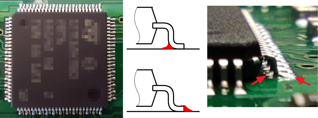
If there is a solder bridge from reflowing, apply some flux to the bridge, then get an iron and clean up the bridge. Usually the solder will move to either pin and leave the bridge. Excess solder may need to be removed (if there is too much of it) with multiple passes with a tip or with solder wick.
There are a few methods listed here:
http://store.curiousinventor.com/guides/Surface_Mount_Soldering/QFP
In summary of the link above one can drag small amounts of solder across the QFP pins with sufficent flux the pins can be wetted with no bridging. These methods also apply to removing bridges.
Another note:
With flow or reflow, it's better to stop a problem before it starts. Keep things clean and consistent. If reflowing a part, remove as much solder from the pads if your going to apply paste. If your not going to apply paste, it can also be good to remove most solder from the pins and make them look consistent. If you do this the reflowing process will be better.
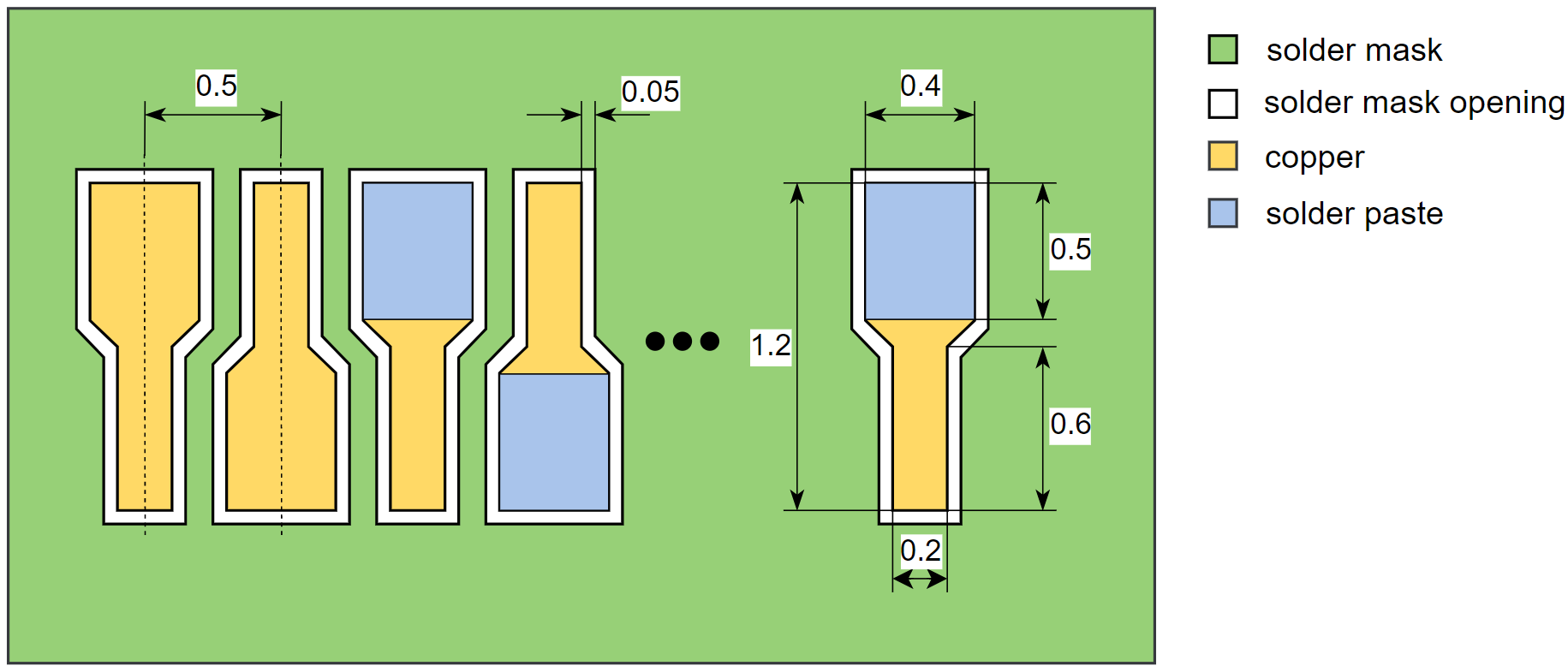
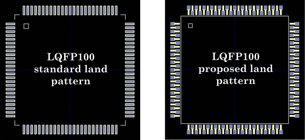
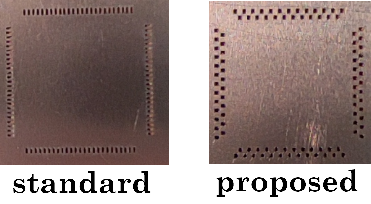
With any paste soldering if you don't have the right solder and the correct amount, you'll get bridges. If you clean off the pads well, and use a good process then you won't get bridges. You apply the correct amount with the right sized stencil, and must be sized around the pads. Use the recommended stencil pattern and thickness:

The thickness of the stencil determines the amount of solder paste
deposited onto theprinted circuit board land pattern. Due to the fine
pitch and small terminal geometryused, care must be taken when
printing the solder paste on to the PCB. Typical stencil thicknesses
are given in Table 3
Since QFN/SON are (most likely) not the only package on the actual
production PCB,the recommended stencil thickness for the other
packages may be thicker than desired.For such a case, a step-down
stencil is recommended, where most of the stencil for thePCB has a
typical thickness, but the area for the QFN/SON would be reduced to
100 to150 μm, depending on the package pitch.
The dimension of the stencil openings should be a minimum 25 to 30 μm
(5 to 10 %)smaller than the size of the corresponding copper lands to
account for alignment and PCB tolerances. A fillet at the corners
reduces the adhesion to the solder paste and improves the paste
release (Figure 24). The fillet radius depends on the solder
pastetype; i.e. it should be larger than the diameter of the solder
spheres.
A minimum aperture size is needed to ensure the proper release of the
solder paste during stencil printing (Figure 24). The area ratio and
the aspect ratio between stencil opening and stencil thickness are
used to determine the minimum dimensions,respectively.

Source: https://www.nxp.com/docs/en/application-note/AN1902.pdf


