I'm trying to power my circuit via a wireless coil module and have a working circuit using a desktop voltage supply at the same voltage (12V). Simply by swapping out the desktop voltage supply with the wireless coil module results in vary unexpected differences in voltage and current within the circuit. I am looking for any possible explanations as to why this could be occurring and how I could verify such an explanation via some test scenario.
I have a more complex circuit, but in order to debug things, I've disconnected everything down to the most minimal example where this problem still persists and present the debugging steps I've tried in the block diagrams below. Although the use of these two voltage regulators is not apparent in these block diagrams, I need them for other parts of the circuit that I've disconnected for clarity here.
All of these voltage regulators and charging modules are premade modules, and I don't have any circuit diagrams for any of them and there are a ton of micro surface mount components, so reverse engineering it would take a fairly extensive amount of work, and I would likely irreversibly break some things along the way, so hoping to avoid this. I've linked to the purchase page I used for each module when I mention them below.
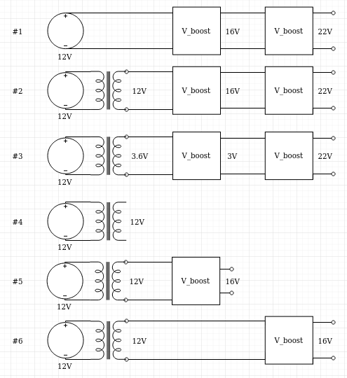
- "#1" Shows the working diagram using just the desktop voltage supply
- "#2" Shows what I would expect to occur by simply adding in the wireless coil (note I used a transformer icon for lack of a better one).
- "#3" Shows the actual voltages. I also note the current draw after the wireless coil jumps from 30mA to above 1A!
- "#4" I eliminated everything in the circuit to test just the coil output voltage. Works as expected.
- "#5" Adding in the first voltage regulator V_boost also works as expected.
- "#6" Removing the first voltage regulator results in normal operation again.
It seems there is something in the wireless charging module that conflicts with the operation of the two voltage regulators in series. Is there something inherently wrong with connecting two buck/boost regulators in series? Do switching frequencies need to be mismatched or something such that I am running into something like positive/negative interference of the waveforms?? I'm grasping at straws here, but this is as far as I'm able to debug this without some further knowledge regarding the inner workings of these regulators and wireless coil modules. Hoping someone can enlighten me or ask some leading questions that would lead to a good test to run.
Edit1:
I swapped out a few other buck and boost regulators to find that this problem only seems to occur when putting two boost regulators in series. The ones I tested:
Does this hint at anything further?
Edit2:
Based on further testing I concluded that the previously mentioned R_L can be excluded and V_buckboost could be replaced with an identical V_boost to still recreate the issue with a more minimal working example. I've edited the block diagrams and original question text to reflect these changes.
Upon request, here are the closest things to schematics I could find based on the seller info and what part codes I could make out under a magnifying glass. These are datasheets with a few example schematics inside.
- The wireless charging module though I could only find this is Chinese. A possible alternative chip according to this which mentioned this and a XKT-510 chip interchangeably shows a similar example circuit and use scenario. See here for that datasheet (see page 4 of 5 for example circuit)
- The V_boost (see page 3 of 8)
Although I couldn't find anything in English about the actual wireless charging module chip, based on this it looks like it combines a AC/DC rectifier with a voltage regulator. I tested the leads of the coil vs the output on the module using a scope, and this looks like a sensible explanation.
Finally, a fairly key discovery I just tested was adding a 1000uF capacitor over the input of the 2nd V_boost and tested the behavior.
At first connection, the same issue of over current draw and strange voltages appeared, but after disconnecting, and connecting again (by complete chance) I noticed that everything worked as expected. Observing the scope, showed that voltages over the input of the 2nd V_boost were rising and dropping quite slowly due to this capacitor (as expected), and it seems that if the circuit is started when the input voltage over the 2nd V_boost is high enough (>300mV or so) then the circuit will operate as expected. If you let the capacitor drain any further than this, and try again, it will fail. And by fail, I mean regardless of how long you wait, it will stay in this failed state, drawing about 1.1A, and I burnt through one of my 600mA rated wireless transmitter chips in the process. So it seems I have to find a way to provide some initial voltage at the input of the 2nd V_boost in order for it to initialize something properly.
I'll have a look into the datasheets of the V_boost chips a bit more. Maybe there is some safety feature that is shutting things down when it sees a current draw at low voltage or something. I'm also still dumbfounded as to why the tabletop supply does not run into this issue. Will keep troubleshooting. Thank you for everyone's helpful comments so far!


