0
\$\begingroup\$

I am reading the data sheet of the 78xx regulators and they say the maximum input voltage is like 40 V. Seems like it didn't have different maximum values depending on the output voltage, '05, or '12, or '15. But usually the designs show input voltage some amount over the desired output voltage, but not excessively much.

What if, for example, I have 12 DC input supply voltage and I just slam a 7805 regulator in to get 5 V output? Will it then just short 7 V to ground in order to maintain the 5 V under load? E.g., if I want to use the full 1.5 A that they are rated at, does that mean that it "shorts" 1.5 A at 7 V = 10.5 W of power straight to the ground, getting all hot?

Or is that safe and it uses some other way to reduce the voltage without wasting so much energy and not going up in smoke?

\$\endgroup\$

4 Answers 4

6
\$\begingroup\$

Will it then just short 7 V to ground in order to maintain the 5 V under load?

It doesn't short anything to ground, but besides that you got it right. If the input is 12V and the output is 5V then you'll have 7V across the regulator. Since the load current goes through the regulator, it will dissipate according to P=IV. So if you got 1.5A and 7V across the regulator, then indeed it will dissipate 10.5W and require a heat sink.

For better efficiency, at this kind of high current it is much more convenient to use a switching regulator. For example you can use these ready-made ones which are very simple to apply, just read the datasheet and add the required input/output caps. If you wonder what's inside, these show the internal schematic in the datasheet. There's also a search engine.

At the rated efficiency of 90%, losses are 10% so with an output power of 5V*1.5A=7.5W the switching regulator will dissipate only 0.75W, which means you don't need a heat sink. It is more expensive than a 7805 but when you compare to the cost of a 7805 plus a large heat sink, it's a much better solution. Also it will draw much less current from the input.

\$\endgroup\$
4
\$\begingroup\$

@bobflux has addressed the power dissipation question.

I am reading the data sheet of the 78xx regulators and they say the maximum input voltage is like 40 V. Seems like it didn't have different maximum values depending on the output voltage, '05, or '12, or '15. But usually the designs show input voltage some amount over the desired output voltage, but not excessively much.

enter image description here

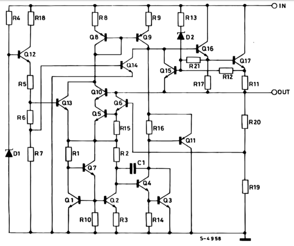
Figure 1. The internals of a 7805. Image source: ElecCircuits.

Don't forget that the regulators have one pin connected to 0 V (ground) so the input voltage isn't just between input and output. That would explain why the maximum input voltage remains fairly constant for the range of output voltages.


Where is the voltage dropped and the power dissipated?

Without digging too deeply we can see that Q17 is the regulating transistor. Almost all of the output current will pass through Q17 to OUT. If you like, the rest of the chip controls the resistance of Q17 to regulate the output so that constant voltage is maintained.

While we're here we can note a couple of other points.

  • Q16 and 17 together form a Darlington pair and they'll drop a minimum of 1.4 V between IN and OUT.
  • As the output current increases the voltage drop across R11 increases. As it approaches 0.6 to 0.7 V Q15 will start to turn on and this will steal the bias away from Q16 turning the Darlington pair off enough to limit the current. If your device has a 1.5 A current limit then R11 must be about 0.65 / 1.5 = 0.43 Ω.
\$\endgroup\$
4
\$\begingroup\$

Overview

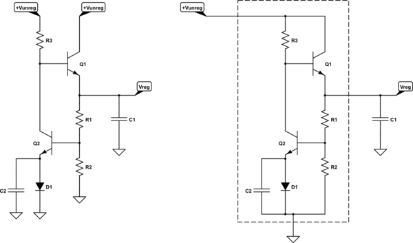
It may be easier to understand a linear regulator by seeing a simplified schematic of one:
schematic

simulate this circuit – Schematic created using CircuitLab

(IC regulators are much more sophisticated. For example, the above schematic has no short-circuit protection, no thermal protection, and its output voltage will vary with the ambient temperature -- to name just a few of its problems. That said, it does actually regulate the output voltage.)

Discussion

On the left is just the bare schematic. On the right, I put a little box around it so that you can more easily see the three terminals of a 3-terminal regulator and what's inside and outside of this simplified version of one.

\$Q_1\$ does the actual job of dropping voltage from the unregulated power supply rail (called \$V_\text{unreg}\$ above.) It's collector is nailed to the unregulated supply, but its emitter voltage is the regulated output. Because of that fact, almost all of the needed dissipation takes place in \$Q_1\$ since all of the load (not shown) current must come through \$Q_1\$ and \$Q_1\$ will be controlled by the rest of the circuit shown so that it drops just the right amount of voltage to perform the regulation job.

Resistor \$R_3\$ supplies the needed base current for \$Q_1\$ (plus a little more.) Resistors \$R_1\$ and \$R_2\$ provide a simple voltage divider that divides the regulated output voltage (\$V_\text{reg}\$) by some desired factor. So the node wire between \$R_1\$ and \$R_2\$ present a fraction of the regulated voltage to the base of \$Q_2\$. Meanwhile, the emitter of \$Q_2\$ "observes" the diode voltage of \$D_1\$ (which is presumed to be relatively constant regardless of changes in the current through it) and compares it with the base voltage provided by the resistor divider pair.

If the voltage at the resistor divider pair increases, this causes \$Q_2\$ to increase its collector current. But that causes a larger voltage drop across \$R_3\$ and that pulls downward on the base of \$Q_1\$ (which causes its emitter to similarly move downward.) This change "corrects" the output voltage by lowering it and that causes the voltage at the resistor divider pair to return to where it should be.

If the voltage at the resistor divider pair decreases, this causes \$Q_2\$ to decrease its collector current. But that causes a smaller voltage drop across \$R_3\$ and that pulls upward on the base of \$Q_1\$ (which causes its emitter to similarly move upward.) This change also "corrects" the output voltage by raising it and that causes the voltage at the resistor divider pair to again return to where it should be.

That's how it works. But the basic answer to your question is that \$Q_1\$ is continually adjusting itself (via this closed loop circuitry arrangement) so as to maintain the regulated output voltage. It does this by dropping more or less voltage across itself (between its collector and emitter.) And since the entire load current must pass through \$Q_1\$, its dissipation will be the product of this voltage drop times the load current (plus a little extra for the base current component.) It's not quite like you write it (shorting it to ground.) But I suppose your writing gets a point across.

(It's not terribly important for this discussion but some added dissipation also occurs in the surrounding circuitry. For example, \$R_3\$ may dissipate 10% as much.)

Summary

Linear IC regulators work similarly to the above. They just do so with much better circuitry designed to handle a host of problems that users commonly want addressed. These are things like providing a precision output voltage that doesn't vary much with ambient or operating temperatures, doesn't age over time, is relatively immune to unregulated supply voltage variations and ripple, won't explode or burn up if someone uses a screwdriver to short the output to ground, etc. The usual things people expect from a good regulator.

\$\endgroup\$
0
\$\begingroup\$

The internal transistors must be isolated form the underlying silicon substrate.

The failure voltage does not vary as the Vregout varies.

Its called collector_bulk breakdown, or drain_well breakdown.

\$\endgroup\$

Your Answer

By clicking “Post Your Answer”, you agree to our terms of service and acknowledge you have read our privacy policy.

Not the answer you're looking for? Browse other questions tagged or ask your own question.