-2
\$\begingroup\$

I was wondering if somebody could help in explaining to me what information the following two schematic diagrams show.

I am quite new to this so I would appreciate if someone could help me understanding the basics.

For example, why are the capacitors placed where they are?

What an MPU CLK? MPU SIMO ?

\$\endgroup\$
4
  • \$\begingroup\$ Did you try to type the part numbers for the IC's in Google and check the datasheet for them? MIC5219-3.0YML and MPU-6000 \$\endgroup\$
    – jippie
    Commented Dec 23, 2012 at 22:46
  • \$\begingroup\$ The entire data sheet is 6 pages. Should I put the whole thing on here? I guess my main question is how does someone go about putting the pieces together? \$\endgroup\$ Commented Dec 23, 2012 at 23:20
  • \$\begingroup\$ @user1068636 Link to the datasheets somewhere (e.g. the sites where you took them from). \$\endgroup\$
    – Renan
    Commented Dec 24, 2012 at 0:48
  • \$\begingroup\$ Why did you flag your own question? Do you want to have it removed? You can also edit it, if you think it can be turned into a good question. Then we can also reopen it. \$\endgroup\$
    – clabacchio
    Commented Dec 24, 2012 at 10:52

3 Answers 3

6
\$\begingroup\$

I think your question is part of a much larger one - i.e. how to get started with datasheets and schematics in general (or something along those lines)

Basically, the answer is to read a lot, and re-read a lot too. Eventually you begin to recognise common pin names, functions, component uses (depending on context - components may have many uses depending on situation)

Acronyms you become familiar with are things like SIMO (Slave In, Master Out - you will also see MOSI, MISO, or SDI, SDO, SCK, etc - these all refer to the SPI standard. Check the first paragraph of link for naming conventions)
In this case the MPU_CLK is the SPI clock, we can tell because it is connected to the SCK pin, which is the SPI clock pin for the IC. The SIMO is connected to SDI, which means Serial Data In (the alternative naming convention to the MOSI/MISO mentioned above and in the Wiki link)

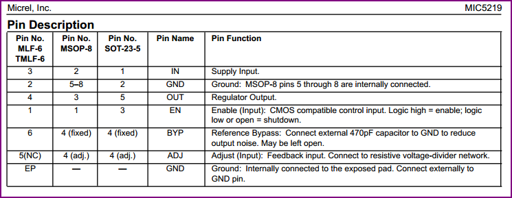
So, for the direct answer, everything is in the datasheets for the two chips, specifically these two tables:
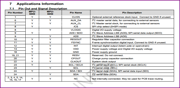
Pin Purpose 1

You can see above that the CPOUT pin is the charge pump capacitor connection (this will be used for an internal boost circuit, often for generating the higher voltages necessary whilst programming e.g. a microcontroller/FPGA - in this case it seems it's supplying the X,Y and Z sections with a bias voltage, see clip below) So, this is why the cap is placed there (the datasheet will have details on the value to use.
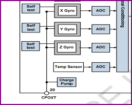
Charge Pump

Pin Purpose 2

The second part of your question is answered basically by the table above, this gives the pin number and description of function.

\$\endgroup\$
4
  • \$\begingroup\$ Hi Oli - this is exactly what I needed. Awesome answer. \$\endgroup\$ Commented Dec 24, 2012 at 4:09
  • \$\begingroup\$ Also, I'm just a little curious, how can I relate this to writing code for a specific schematic? \$\endgroup\$ Commented Dec 24, 2012 at 4:13
  • 1
    \$\begingroup\$ @user1068636 - if you mean code for a microcontroller based schematic, then I would begin with a simple starter kit (e.g. PIC, Atmel, Arduino, MSP430, etc) and go through all the code examples step by step. Also get a breadboard and when you feel comfortable, build a circuit and do something like expand on one of the examples. When I was starting out I built my PIC circuits using veroboard/breadboard, and just experimented with stuff till I understood it. \$\endgroup\$
    – Oli Glaser
    Commented Dec 24, 2012 at 4:44
  • \$\begingroup\$ Also a general book "Pratical Electronics for Inventors" is worth grabbing - don't be put off by the title, it's an excellent intro to the world of electronics, and has very detailed sections on all the basic components, their variants, things to watch out for, etc. Have a search on here too, there are quite a few similar previous questions with good answers on this subject. If you still have specific questions, then just open another one (read the FAQ to make sure you get the best answers by asking a good question) \$\endgroup\$
    – Oli Glaser
    Commented Dec 24, 2012 at 4:48
2
\$\begingroup\$

Your circuit diagrams are incomplete. Things like A1 MPU CLK are called net names, and all these labels with identical names are attached together ... somewhere ... It can be on the same drawing, it can be on another sheet. There is no way to know what is connected if you don't have the rest of the circuit diagrams.

For capacitor placement in the circuit diagram, it is pretty much convenience to the person who drew it. Some like it to resemble the physical PCB layout, some like it when the diagram just looks nice and tidy. Maybe this question is of some use: Rules and guidelines for drawing good schematics

\$\endgroup\$
1
\$\begingroup\$

To make sense of the diagrams, you will need the datasheets for the devices in there and a larger part of the schematic (one which shows where MPU_CLK, MPU_SIMO etc... connect to). E.g. typing MPU-6000 into Google gives this.

Taking a stab at what's seen on the schematic: SIMO and SOMI are used for SPI communications (Slave In/Master Out and Slave Out/Master In respectively). CLK is the clock (presumably coming from the microcontroller/microprocessor being used) needed for the SPI communcation.

For pin meanings, always read the components' datasheet, the information should be there.

As for capacitor placement, it has no meaning per se on a schematic; it's mostly a designer choice. What matters is the placement on the PCB.

\$\endgroup\$

Not the answer you're looking for? Browse other questions tagged or ask your own question.