0
\$\begingroup\$

I have a problem with our microprocessor.

I had written several programs and I tested them on a STM32vlDiscovery (has stm32f100rbt6 microprocessor.) There were no errors and it worked correctly.

Now I programmed the same program on a new STM32F100RBT6 and unfortunately, the program does not work.

The program was completely downloaded on the STM32 and verified but does not work.

In the debug environment, I saw that all registers were zero, as the microprocessor stopped in the first line of the program.

#include <stm32f10x.h>
#include <math.h>
//------------------
volatile short sinArray[20];
volatile int i=0;

//1000 Hz Sine Wave
void TIM2_IRQHandler(void)
{
    TIM2->SR &=~TIM_SR_UIF;
    DAC->DHR8R1=sinArray[i];
    i++;
    if(i==20)i=0;
}


int main()
{
    RCC->APB1ENR |=RCC_APB1ENR_DACEN;
    DAC->CR |=DAC_CR_EN1;
    RCC->APB1ENR |=RCC_APB1ENR_TIM2EN;
    TIM2->CR1 |=TIM_CR1_ARPE;
    TIM2->ARR=199;
    TIM2->PSC=5;
    TIM2->DIER |=TIM_DIER_UIE;
    NVIC_EnableIRQ(TIM2_IRQn);
    TIM2->CR1 |=TIM_CR1_CEN;
    
    //TIM2->SR &=~TIM_SR_UIF;


    for ( i=0; i<10; i++)
    {
        sinArray[i]=(128*sin(i*3.14/10)+127);
    }
    i=0;


    while(1)
    {
    }
}

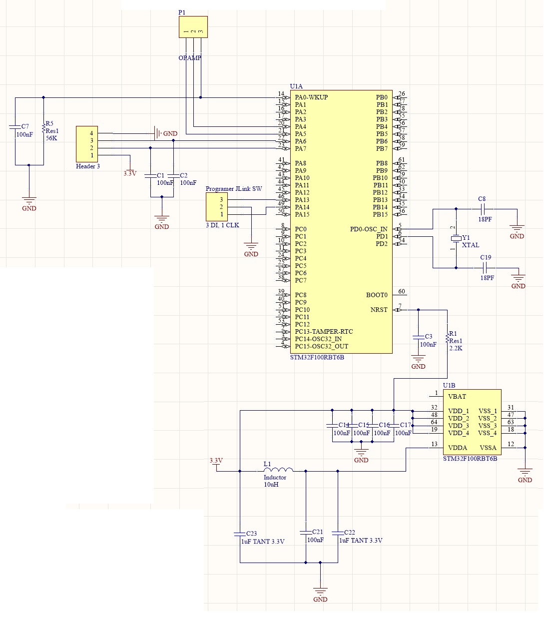
enter image description here

\$\endgroup\$
4
  • 1
    \$\begingroup\$ What have you done so far to debug it? I want to avoid saying things you will only respond that you tried it already. My second question is, why the schematic for important pins is not done according to datasheet and reference desings and discover board schematics? \$\endgroup\$
    – Justme
    Commented Dec 1, 2020 at 18:59
  • \$\begingroup\$ Dear Justme, I connected the BOOT pin to +3.3 with a resistor and it is not in my schematic, I did this later \$\endgroup\$
    – Hossein
    Commented Dec 1, 2020 at 19:30
  • \$\begingroup\$ Why did you not say that in the first place, that is the problem! \$\endgroup\$
    – Justme
    Commented Dec 1, 2020 at 19:32
  • \$\begingroup\$ excuse me for my mistake, I have forgotten to change my schematic, you are right. \$\endgroup\$
    – Hossein
    Commented Dec 1, 2020 at 20:14

1 Answer 1

2
\$\begingroup\$

Connecting BOOT0 to +3.3V which you explained but not shown in the schematics causes the MCU to always go run the factory bootloader after reset, so it will never run the program you programmed.

BOOT0 must be low to run normally.

Also the other issues should be fixed:

-VBAT must not be left unconnected.

-NRST pull-up resistance is unnecessarily low in value. It is not even recommended.

\$\endgroup\$
3
  • \$\begingroup\$ Thank you for your guidance. so after programming, the BOOT0 must be pulled down? \$\endgroup\$
    – Hossein
    Commented Dec 1, 2020 at 19:39
  • \$\begingroup\$ BOOT0 must be low to run your program regardless of how you program it. \$\endgroup\$
    – Justme
    Commented Dec 1, 2020 at 19:57
  • \$\begingroup\$ Basically you'd only have BOOT0 high to enter the bootloader, either if you wanted to use that rather than SWD to load code, or if you were trying to prevent bad code (say code that reconfigures the SWD pins as GPIOs) from running so that you can use SWD to change it. \$\endgroup\$ Commented Dec 1, 2020 at 22:57

Your Answer

By clicking “Post Your Answer”, you agree to our terms of service and acknowledge you have read our privacy policy.

Not the answer you're looking for? Browse other questions tagged or ask your own question.