0
\$\begingroup\$

How to switch best between two voltage sources (5V & 3V3) for a "load" (e.g. a sensor in the application field or Arduino/Raspberry Pi/etc.). The basic setup is as follows: there are two voltage sources: 5V and 3V3 and based on a MCU OUTPUT should either be supplied with the 5V supply or 3V3 supply. The MCU is a 3V3 system.

I thought of basically two ways (following). The question is, if they are correct and which one might work better (although hard to answer generally, question is for "rule of thumb"). The requirements are roughly: design as simple as possible, no fast switching required (e.g. max. once per minute or even less).

A) Using transistors
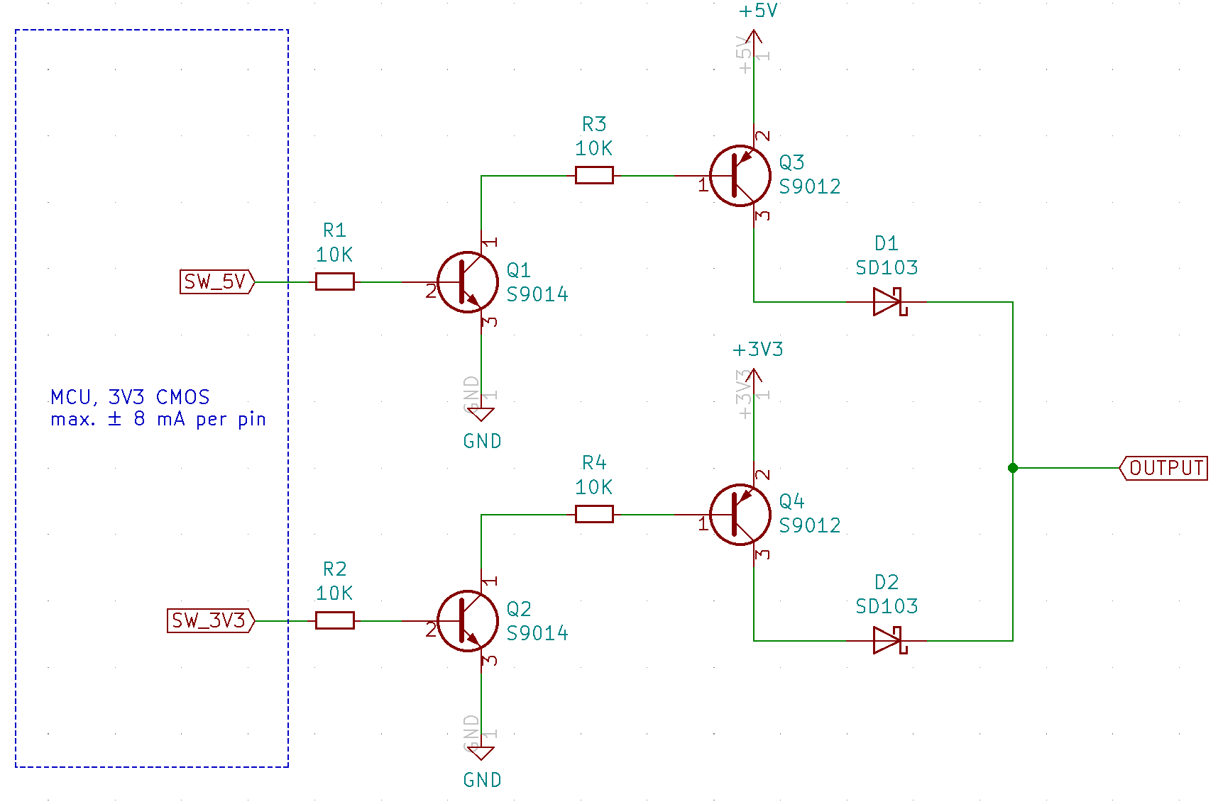
Description: Basically two PNP ("high side switches") are used to switch the 5V/3V3 to the output. In order to keep the PNP off the voltage at the base is going to be nearly at the 5V level and this would "overload" the MCU, so an intermediate NPN stage is driven by the MCU which drives the PNP. In order to protect "reverse voltage" a diode has been added (D1 and D2).

The question is, if this would work (I'm not sure regarding Q1 and Q2) and also the diodes reduce the VCC by ~ 400 mV, so OUTPUT would be 4.6V/2.9V, right? This will cause other "trouble" down the road since the OUTPUT should be proper 5V/3V3. A quick solution could be by increasing the 5V/3V3 accordingly. But the max. system voltage is 5V, therefore a boost converter is also required. Any better ideas here?

B) Using a relay
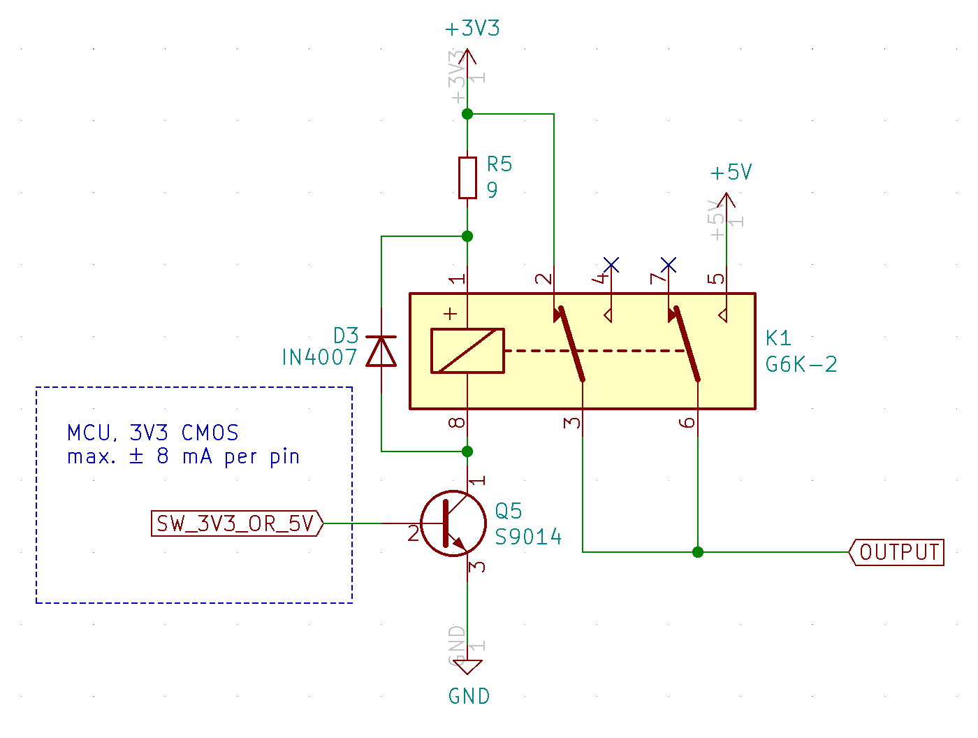
e.g. G6K-2F-Y-TR-DC3 Description: relay limiting resistor (R5) is calculated by dividing the required voltage drop (0,3V: 3V3 -> 3V of relay) by the current of the relay (33 mA). But this solution has mechanical implications (e.g. lifetime)

Edit: it seems that I left out important details:

  • Imax (load) V tolerance? up to 75 mA and ± 10% for both rails (5V/3V3).
  • Use-case: the user can plug in different sensor boards (imagine temp sensor, light sensor etc.), everything digital, the MCU knows which device by user input and based on this switches the defined VCC

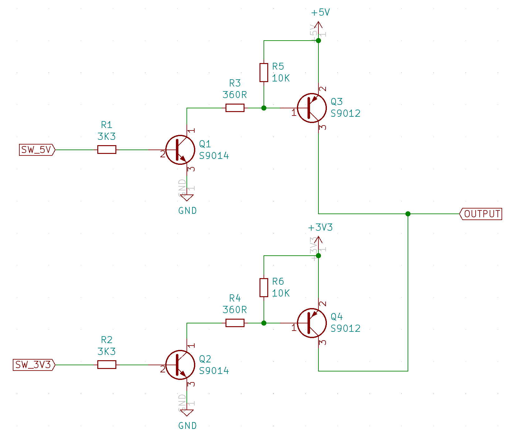
Edit 2: based on the extensive answer of AnalogKid I redraw the schematic of A) just in case anyone want to see it (@AnalogKid thanks for giving so much detail):
\$\endgroup\$
13
  • 3
    \$\begingroup\$ Neither a) or b) until you define V tolerance at I max of TBD sensors \$\endgroup\$
    – D.A.S.
    Commented Apr 6, 2021 at 12:48
  • 3
    \$\begingroup\$ Just to confirm that this is not a XY problem, may I ask why is switching of sensor supply between 5V and 3.3V needed in the first place? How would the MCU know which supply to select? \$\endgroup\$
    – Justme
    Commented Apr 6, 2021 at 12:48
  • \$\begingroup\$ We assume you know which devices need Which voltages between sleep to a downstream Mux address, but you must say the loads \$\endgroup\$
    – D.A.S.
    Commented Apr 6, 2021 at 12:49
  • \$\begingroup\$ If you ask for the "best" solution, you have to list the features that you want and give them priorities. The "best" is of course the "ultraconduct-idealswitcher 2020-12" but yeah, it costs more than € 173000, are you willing to pay that? (Yes, I made this up). But this solution has mechanical implications (e.g. lifetime) No, it does not until you prove that it does and that your application needs a longer lifetime than a good relay can offer. \$\endgroup\$ Commented Apr 6, 2021 at 12:51
  • 4
    \$\begingroup\$ And, how fast/how often do you need to switch between 3.3V and 5V? Relay might be the "best" solution if you only have to switch occasionally, and are ok with relay contact bounce and 10 ms switching time. \$\endgroup\$
    – SteveSh
    Commented Apr 6, 2021 at 13:01

2 Answers 2

1
\$\begingroup\$

Your 10% tolerance on 5V= 500mV with 75mA max load means load regulation error from 5V has a max source resistance of 500/75=6.7 Ohms

So I would look for a switch with 2 Ohms saturation Rce in BJT or conduction with FET or CMOS transparent switch operating from 5V supplying 5 or 3V3 to each load.

A PN2222A is 2 Ohms typical Rce and 4 Ohms max.
The 2N290x series is 4 To 5 Ohms for Rce = Vce(sat)/Ic. When using Ic/Ib=10.

I would prefer 5% tolerance.

so I filter D-K’s selection if “active” Analog Mux switches from >1k results to normally stocked and in-stock to many duplicate results that gave a maximum of 5.5V and min. <3V and get 576 results.

From this I chose a random <2 Ohm a quad SPDT Analog Switch circuit that features Break-before-make and low voltage control.

DG2525 Vishay Siliconix.
0.37 Ohm Low THD and Capacitance, Dual DPDT / Quad SPDT Analog Switch $0.77/pc 3k reel

Design time selection: 5min + 15 min.typing this answer .

Now you can select power and signal with 1 switch. With unused input set to a Vref of your choice for self test.

Be sure to limit load capacitance on sensors . You can compute that ok?

\$\endgroup\$
1
  • 1
    \$\begingroup\$ I followed your path and found the ADG819 or ADG888 which I quite like (solder friendly package); I think using an analog mux switch is the best solution between a discrete circuit and a mechanical relay. For limiting the cap. load I'ld add a series resistor to limit that initial inrush current. One question: can the analog switch be powered by the 3V3 rail and switch the higher 5V rail? Where do I get this info from the datasheet? \$\endgroup\$
    – mythbu
    Commented Apr 7, 2021 at 8:42
2
\$\begingroup\$

I would go with the transistor version. It consumes less power, generates less electrical noise, and allows a state when the sensor is completely unpowered. However, the design needs work.

  1. Add pull up resistors from the Q3 and Q4 transistor bases to their emitters. This assures a fast and complete turn off. 10K should be fine.

  2. Decrease R3 and R4 to 360-470 ohms. For 75 mA collector current you need around 5-7 mA of base current for firm saturation.

  3. Decrease R1 and R2 to 4.7 K or less, again for firm saturation.

  4. Delete D1 and D2. The transistors provide enough off isolation by themselves, and deleting the diodes increases the output voltages to within 0.1 V of the source voltages.

  5. You might want to add some decoupling capacitance on the switched output, but that is a tradeoff between filtering noise and adding a delay to the time it takes to switch from the 5 V output to the 3.3 V output as that capacitance discharges by 1.7 V.

\$\endgroup\$
3
  • \$\begingroup\$ Thank's for the details analysis. I updated the question with a schematic for it! \$\endgroup\$
    – mythbu
    Commented Apr 7, 2021 at 8:54
  • \$\begingroup\$ R6 and R7 - base to emitter. \$\endgroup\$
    – AnalogKid
    Commented Apr 7, 2021 at 11:44
  • \$\begingroup\$ Fixed (sorry for that) \$\endgroup\$
    – mythbu
    Commented Apr 7, 2021 at 20:11

Your Answer

By clicking “Post Your Answer”, you agree to our terms of service and acknowledge you have read our privacy policy.

Not the answer you're looking for? Browse other questions tagged or ask your own question.