I have been reading that a photodiode is built by sandwiching a very thin N type semiconductor togther with a thicker P type. Why is that so?
-
\$\begingroup\$ I suspect a significant point has been missed. The backside layer of a planar photodiode is thin because the diffusion time for carriers generated outside the depletion region are really slow. Like three orders of magnitude slower than when generated in the depletion region. With speed being is part of almost product goal, this slower diffusion mechanism has to be mitigated! This is either done by a thinner backside layer or else an intrinsic layer, in between (PIN diode.) \$\endgroup\$– jonkCommented May 6, 2021 at 0:15
2 Answers
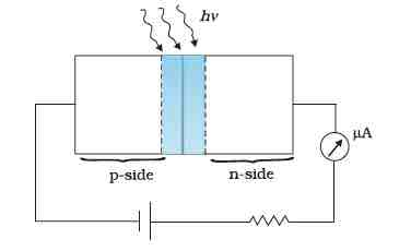
The texbook photo:
doesn't represent the real physical situation. I mean the actual sizes of the layers in relation to oneanother.
It is a simplified view that helps to explain what is happening in a PN junction.
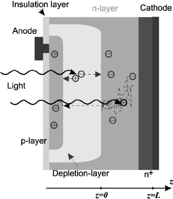
This is a more realistic presentation:
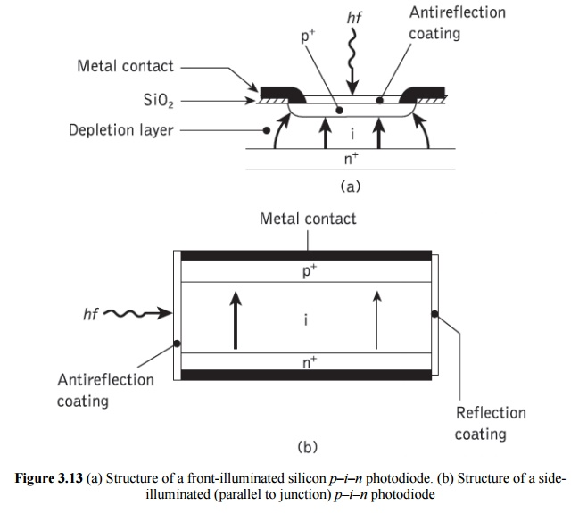
This is another more realistic sideview drawing:
The reason why the N-type layer is much thinner than the P-type layer is due to the fact that the manufacturing starts with a P-type wafer.
N-type doping is then implanted into that P-type wafer which will turn a thin surface area of that P-type wafer into N-type.
In these drawings the P-type layer is much thinner than the N-type so the opposite of what you stated (N-type is thinner). Actually that doesn't matter, the manufacturer starts with the thick layer and then add doping to make the thin layer.
If you start with a P-type wafer, after adding N-type doping you will get a thin N-type layer.
If you start with a N-type wafer, after adding P-type doping you will get a thin P-type layer.
But it was P-type? Where did the all the P go?
Good question! If the doping of the N-type is higher than than the existing doping of the P-type it will overrule that doping. The P-doping is still there but "overwhelmed" by the N-type, making the surface N-type.
I’ll answer your 2nd question.
The battery is used here to reverse bias the PD for lower leakage current and lower junction capacitance. Then the voltage across the bias R to gnd. measures the current.
Others make prefer to use 0V bias and measure the conduction voltage with different characteristics. This is more sensitive but also more non-linear impedance for large variations.


