3
\$\begingroup\$

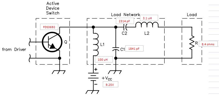
I'm having issues getting a Class E Amplifier to work properly. I designed the amplifier based off of Nathan Sokal's paper titled "Class-E RF power amplifier"

https://people.physics.anu.edu.au/~dxt103/calculators/class-e.php

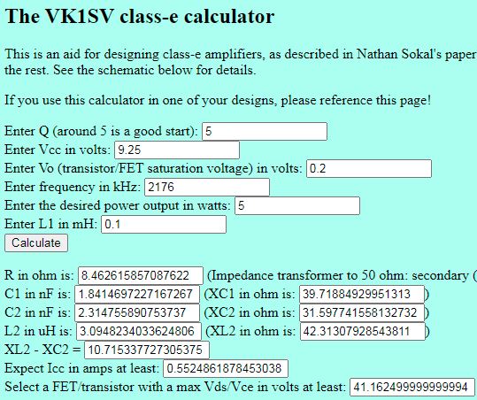
I designed for a 5 Watt amplifier at 9.25 volts:

enter image description here

enter image description here

enter image description here

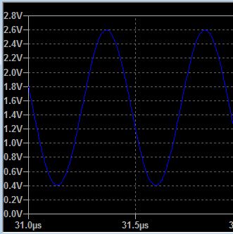
My input signal is a 2.176 MHZ signal with a peak-to-peak amplitude of 2.2V and an offset of 1.5 Volts

enter image description here

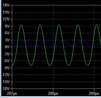
When I run the SPICE simulation with that continuous sine wave signal, there are no issues and the amplifier appears to be working properly (blue is input signal, green is output signal from the amplifier).

enter image description here

The issue starts when I try changing the input signal from a continuous signal to a burst signal. The burst signal I am trying to amplify is the same 2.176 MHZ, 2.2V peak-to-peak amplitude and 1.5V offset. It is continuous for a certain amount of time, off for 7 us, then continuous again and this repeats.

enter image description here

Same input signal, just zoomed out enter image description here

The problem is that the output amplified signal seems to over shoot and gradually fall back down to its proper voltage.

enter image description here

enter image description here

I don't know why it is overshooting. It works perfectly fine when the input signal is continuous. I also built a physical model of this amplifier and got similar results.

One last interesting thing I noticed is the current at L1 seems to be taking too long to reach its steady state value (L1 current in red below). From the looks of it, if it reached its steady state much quicker, the amplified signal wouldn't overshoot.

enter image description here

Anyway I'm out of ideas so I thought I would reach out here. It seems to me like this is probably a common issue with trying to amplify burst signals and hopefully there is a common solution. Thanks everyone!

\$\endgroup\$
5
  • \$\begingroup\$ Not sure if this will help, but a couple of clarifying questions here: (1) Did you add ESR to the inductors? (2) How did you get 0.2V for the "saturation voltage" of the FET? (3) isn't the whole point of using the gate driver IC to use the BOOST pin with a bootstrap diode? (4) Did you try driving the gate directly with an ideal source and without the LTC4440A-5? (5) Did you try replacing the FET with an ideal switch to see what happens? \$\endgroup\$
    – Ste Kulov
    Commented Aug 9, 2021 at 6:41
  • 1
    \$\begingroup\$ What does the signal look like at the gate of the FET? If it follows the same pattern, then the issue is in the LTC4440A, if not, then the issue is in the output network. \$\endgroup\$
    – Aaron
    Commented Aug 9, 2021 at 13:55
  • 2
    \$\begingroup\$ Your last plot (very useful, thanks) shows I(L1) increasing in the inter-symbol periods, when power output is zero. This suggests that your transistor is ON, when it should be OFF. \$\endgroup\$
    – glen_geek
    Commented Aug 9, 2021 at 14:24
  • \$\begingroup\$ Hello Aaron, the signal at the gate of FET does not follow the same pattern. It is a square wave 9.25V as expected, so the issue as you have suggested is the output network. Thanks for your comment. \$\endgroup\$
    – Dustin
    Commented Aug 9, 2021 at 16:08
  • \$\begingroup\$ Hello glen_geek, I think you are on to something. I plotted the square signal at the MOSFET gate. The signal itself is good (9.25V square signal as expected). But during the off periods between bursts, the gate voltage is ON at 9.25V causing that current to increase when it should be OFF. I will look into this further and let you know. Thanks! \$\endgroup\$
    – Dustin
    Commented Aug 9, 2021 at 16:14

1 Answer 1

1
\$\begingroup\$

I have seemed to find a solution and thought I would post it in case anyone else has a similar issue.

enter image description here

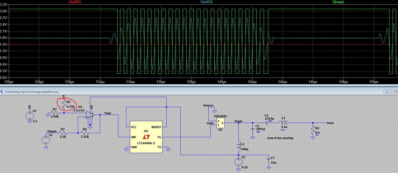
The problem was with the setup around the comparator (LT1719) U3 at the beginning of the circuit. The - pole of U3 was being fed 1.5 volts (determined by values of R1 and R3) which is shown as the teal trace Vn003. The + pole of U3 is the input signal, Vn002 red trace. During the off period, the signal low point was around 1.8 volts, which is greater than 1.5 volts it was being compared to, so it outputs HIGH. I simply had to alter the value of R1 to give me 1.8 volts being fed into the comparator, instead of 1.5 volts. This solved the issue.

\$\endgroup\$
1
  • 1
    \$\begingroup\$ How much current does the MOSFET draw between signal bursts? \$\endgroup\$ Commented Aug 9, 2021 at 20:32

Your Answer

By clicking “Post Your Answer”, you agree to our terms of service and acknowledge you have read our privacy policy.

Not the answer you're looking for? Browse other questions tagged or ask your own question.