0
\$\begingroup\$

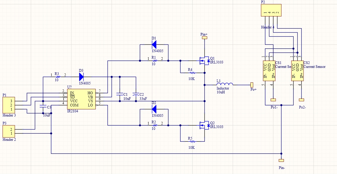
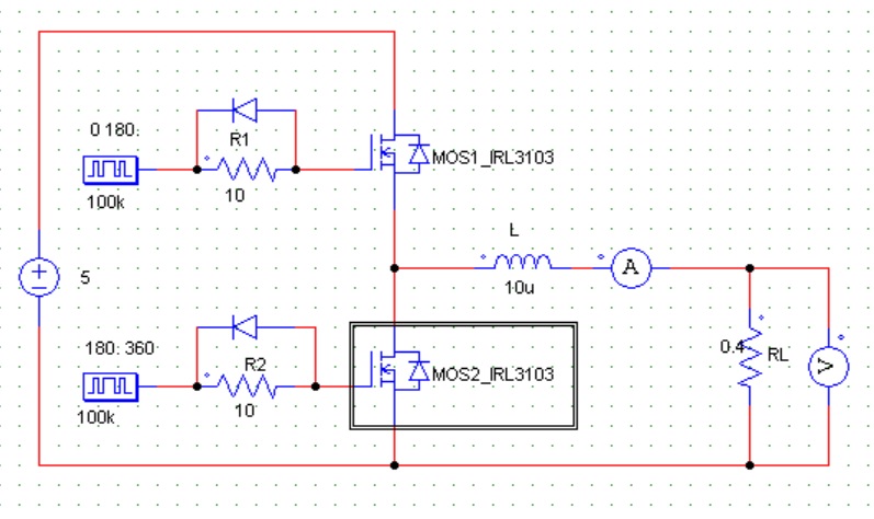
I am going to measure the electrical response (voltage drop vs current) of an electrical contact joint modeled as resistance 0.4 ohm in following figure. I made a prototype circuit to control the current through the electrical contact joint and measure the voltage drop. The schematics was attached, too. The MOSFETs IRL3103 are switched using gate driver IR2104. The inductor was made of ferrite core. The problem is high loss and high temperature in first MOSFET. How can I minimize the power loss in the first MOSFET?

The actual voltage is 5V and the measured current for 50% duty cycle is 6A. The inductor was not saturated in 6A.

enter image description here

enter image description here

\$\endgroup\$
3
  • \$\begingroup\$ The irl2104 won’t work too well on 5V. Your mosfet is probably not driven correctly. Please provide a schematic so we don’t have to guess or play 1000 questions. \$\endgroup\$
    – Kartman
    Commented Aug 17, 2021 at 7:41
  • \$\begingroup\$ Your bottom MOSFET doesnt make sense. Not connected to a supply. 100kHz switching requires high current gate drive. 10Ohms slows it too much. Even 0Ohms is too much without a gate driver \$\endgroup\$
    – DKNguyen
    Commented Aug 17, 2021 at 13:54
  • \$\begingroup\$ Dear DKNguyen, The gate driver is IR2104. How much resistor do you recommend for the input gate of mosfets? Does such resistor have effect on the power loss of mosfets? \$\endgroup\$ Commented Aug 18, 2021 at 6:05

1 Answer 1

0
\$\begingroup\$

Vgs of Q1 must >=4.5V using the Vb from the PWM of Q2. Verify Vb and Q2-Vgs when conducting to isolate the problem of higher than expected Vds(Q2) causing heat rise for a 20 mOhm switch.

The 2nd schematic is missing a connection from Q2-S to 0V (Pin-)

\$\endgroup\$
3
  • \$\begingroup\$ Dear Tony Stewart, Thanks for reply, IR2104 was connected to power supply Vcc=12V. Since, the power supply of main circuit is 5V, Vgs of Q1 is approximately 7V. Vds of Q2 is approximately 5V. Negligible temperature rise is sensed in Q2 in the prototype circuit. How should I modify the circuit to minimize the power loss in Q1? \$\endgroup\$ Commented Aug 17, 2021 at 15:39
  • \$\begingroup\$ Verify/Measure 1st, analyze 2nd , modify 3rd. \$\endgroup\$
    – D.A.S.
    Commented Aug 17, 2021 at 15:49
  • \$\begingroup\$ Follow this farnell.com/datasheets/2254418.pdf \$\endgroup\$
    – D.A.S.
    Commented Aug 17, 2021 at 15:58

Your Answer

By clicking “Post Your Answer”, you agree to our terms of service and acknowledge you have read our privacy policy.

Not the answer you're looking for? Browse other questions tagged or ask your own question.