0
\$\begingroup\$

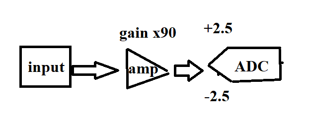
If my signal path is as the following: enter image description here

My input DR is 20mVpp and goes through the above path, and the ADC used is 16 bits. Would the LSB be 5V/(2^16)=76uV or the gain will be added to the LSB as (5V/(2^16))/90=0.84uV. If the gain is added I am having a hard time understanding why it improves the bit resolution.

\$\endgroup\$
1
  • \$\begingroup\$ It depends whether you measure the LSB before or after the gain stage. \$\endgroup\$
    – user16324
    Commented Oct 14, 2021 at 16:00

2 Answers 2

1
\$\begingroup\$

The resolution is still 16 bits in either case, because the resolution is determined by how many bits the ADC is designed to produce; but there can be an advantage to using an appropriate gain stage.

The 90V/V gain stage reduces the effective LSB step size (from \$ \frac{5~\text{V}}{2^{16}}=76~\mu\text{V} \$ to \$ \frac{5~\text{V}/90}{2^{16}}=0.84~\mu\text{V} \$ as you suggest), and also reduces the dynamic range by the gain factor (from \$ \pm2.5~\text{V} \$ to \$ \pm0.02778~\text{V} \$ ).

Reducing the dynamic range at the input is good, when it is a better match to the actual dynamic range of the input, so that more of the ADC's fixed digital range is mapped to useful signal.
\$\endgroup\$
3
  • \$\begingroup\$ Thank you, so since the DR has been reduced to +/-27mV due to the gain stage then I can achieve higher input range than the 20mVpp noted or I can increase the gain up to 250V/V to have a DR of 20mVpp and have an increase in the effective LSB further? \$\endgroup\$
    – Shannon
    Commented Oct 14, 2021 at 8:13
  • 1
    \$\begingroup\$ There should be some margin for calibrating out the gain stage's offset errors and other distortions. Don't count on using the ADC's entire 0-65535 code range, because that guarantees your signal will get clobbered by offset/gain errors. The 90V/V gain stage reduces the ADC's dynamic range to +/-27mVpp/16bits, and you state the signal of interest needs +/-20mVpp, so it sounds like 90V/V is near optimal. More gain will reduce the LSB size (more detail) but also reduces the amount of dynamic range that can be measured; and it's already close to thermal noise limits. \$\endgroup\$
    – MarkU
    Commented Oct 14, 2021 at 10:45
  • \$\begingroup\$ Got it, thank you so much \$\endgroup\$
    – Shannon
    Commented Oct 15, 2021 at 5:30
1
\$\begingroup\$

It is better because amplifying the signal uses a larger range of ADC codes better as the ADC input must operate the 16-bit range over 5V. Indeed 16-bit values in 5V range is 76uV/LSB at the ADC input, so without gain the 20mVpp range is only 262 different values, but due to gain the signal at ADC input is 1.8V which is 23582 ADC values.

\$\endgroup\$
0

Your Answer

By clicking “Post Your Answer”, you agree to our terms of service and acknowledge you have read our privacy policy.

Not the answer you're looking for? Browse other questions tagged or ask your own question.