0
\$\begingroup\$

I have a 24-bit ADC that is controlled by an FPGA. I want to take the ADC input and output it from a 16-bit DAC that is also controlled by the FPGA.

Do I simply ignore the 8 LSB bits of the data and output the upper 16-bits to do this mapping?

Wouldn't that act as a gain on the signal since I am technically shifting 8 left thus multiply the signal by 256?

\$\endgroup\$
4
  • \$\begingroup\$ Decimation = truncating , what dynamic range, rate of change, SNR and sampling rate might determine if a better algorithm like sigma-delta conversion or logarithmic compression or something else is needed. Or not. \$\endgroup\$
    – D.A.S.
    Commented Apr 20, 2022 at 5:49
  • 5
    \$\begingroup\$ Assuming there is no change of VREF (ADC and DAC have same VREF) then discarding the LSB is exactly what you want to do. Full scale on the DAC is VREF, and full scale on the ADC is VREF. 2^24 - 1 is VREF on the ADC, and 2^16-1 is VREF on the DAC. \$\endgroup\$
    – user57037
    Commented Apr 20, 2022 at 6:01
  • \$\begingroup\$ I see, my DAC has a Vref of +/-18V while the ADC has +/-2.5V. This means I would have to multiply the ADC value to be mapped to the DAC range, correct? \$\endgroup\$
    – Shannon
    Commented Apr 20, 2022 at 6:52
  • 4
    \$\begingroup\$ It all depends on your needs, which you know and we don't. If you are handling large signals, ignore the LSBs. If you are handling small signals, ignore the MSBs. If you are handling both ... your choice (which you can dynamically change, if necessary) \$\endgroup\$
    – user16324
    Commented Apr 20, 2022 at 11:57

3 Answers 3

2
\$\begingroup\$

Technically you are not even shifting left by 8 so you are not multiplying by 256. Like you said yourself, the DAC is just ignoring 8 bits because it can't handle them.

So there will not be gain if the ADC at 24 bits and DAC at 16 bits have the same voltage range.

\$\endgroup\$
1
  • \$\begingroup\$ I see, so it would be a gain if I kept for example the 24-bits and shifted left thus the lower LSBs would be zeros. And in this case this is not happening. Got it, thank you \$\endgroup\$
    – Shannon
    Commented Apr 20, 2022 at 6:40
2
\$\begingroup\$

Taking the MSBs of the ADC and routing them directly to the MSBs of the DAC will result in you mapping the nominal full scale range of the ADC to the nominal full scale range of the DAC.

This may or may not be what you want to do.

If you want the whole system to have a gain of 1, then you would need to scale the numbers in your FPGA by the ratio of the full scale ranges.

\$\endgroup\$
2
  • \$\begingroup\$ Got it, my DAC FS is 18V while ADC FS is 2.5V thus the FPGA has to divide the value by ~7.2 to map ADC FS to DAC correct? if so, is this division feasible with FPGA or it will take a lot of resources? \$\endgroup\$
    – Shannon
    Commented Apr 20, 2022 at 10:12
  • 2
    \$\begingroup\$ Yes, your numbers are correct. However, we never divide in hardware if we can help it, always multiply, so by 1/7.2 = 0.1389. However, that's very close to 0.125 (1/8) which we can get with a 3 bit right shift, which costs exactly zero in FPGA resources, if the approximation is good enough for you. If not, then expand 0.1389 as a binary fraction, and add as many terms as you need, at the cost of n-1 adders for n bits. For instance with only two terms, binary fraction 0.001001 = 0.1406 \$\endgroup\$
    – Neil_UK
    Commented Apr 20, 2022 at 11:46
2
\$\begingroup\$

my DAC FS is 18V while ADC FS is 2.5V thus the FPGA has to divide the value by ~7.2 to map ADC FS to DAC correct?

Well, you could do it that way but you'd be losing resolution so, why not just do an analogue potential divider "divide" on the output of your DAC to convert a full scale of 18 volts to a full scale of 2.5 volts.

Most DACs are used to transmit an analogue signal to something that uses that analogue signal and so adding two resistors to the DAC interface circuit seems trivial so, how would you divide by 7.2: -
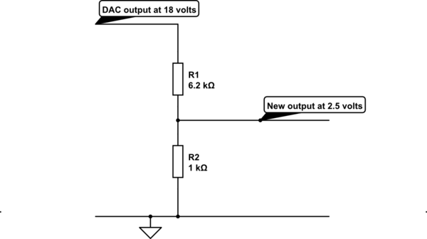
schematic

simulate this circuit – Schematic created using CircuitLab

Regarding your original question, If you handled the top 16 bits (the most significant ones) with a DAC having a reference of 18 volts and you handled the lower 8 bits with a DAC having a reference of 18 volts divided by 65536 (i.e. 0.27466 mV) you could then imagine an analogue adder on the output would perfectly produce a full 24 bit waveform.

But, if you didn't bother with the 8 bit DAC then you are only "losing" resolution in the order of a quarter of a millivolt. Does this make sense as to what is happening by ignoring the lower 8 bits?

\$\endgroup\$

Your Answer

By clicking “Post Your Answer”, you agree to our terms of service and acknowledge you have read our privacy policy.

Not the answer you're looking for? Browse other questions tagged or ask your own question.