0
\$\begingroup\$

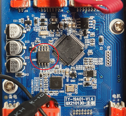
Lets say you have a commercial device you are experimenting with. It has a flash memory chip that cannot be read while in-circuit (I have already tried the clip thing), so you have to de-solder it every time you want to read it, plug it into the socket of the chip programmer, dump the memory, and then re-solder it back onto the PCB, so the device can interact with it.

(I am then doing a diff comparison on the dumps in order to determine how the device's MCU is storing information in the flash chip)

Eventually, after enough heating/cooling cycles, something bad is going to happen to the pads on the PCB. I have ruined a few boards in this way in the past. So I want to minimize the amount of time I am heating it.

I thought "wouldn't it be great if there were some kind of adapter that I can solder onto the SOIC-8 pad on the PCB, that then connects to an SOIC-8 programming socket, so I can easily remove, read, and reinsert the chip onto the board without soldering".

But no such thing exists.

So how do most people handle this situation?

enter image description here

\$\endgroup\$
20
  • 4
    \$\begingroup\$ Why can’t you isolate it from the circuit- at most 6 lines? I can guarantee you just about nobody thinks soldering and desoldering is an acceptable development cycle. \$\endgroup\$ Commented Dec 11, 2021 at 8:09
  • 1
    \$\begingroup\$ ”memory chip that cannot be read while in-circuit” Strange design. Find out what’s pulling it down? \$\endgroup\$
    – winny
    Commented Dec 11, 2021 at 9:16
  • 1
    \$\begingroup\$ A small castellated PCB that can be soldered in place in stead of the SOIC8 chip, with a SOIC8 socket connected to it trough short leads perhaps? \$\endgroup\$ Commented Dec 11, 2021 at 9:23
  • 1
    \$\begingroup\$ If you want to know about what is written to flash, why not use a SPI sniffer to catch the writes? \$\endgroup\$
    – bobflux
    Commented Dec 11, 2021 at 9:39
  • 1
    \$\begingroup\$ Do some research on that PCB, starting with finding the schematic. You may very well find that something - possibly J17 - is a JTAG connector to permit ISP. \$\endgroup\$
    – user16324
    Commented Dec 11, 2021 at 14:04

1 Answer 1

1
\$\begingroup\$

Suggesting that re-designing the device to fit some socket in it isn't an option for you:

  1. You can place a solder jumper (or 0402 0 Ohm) on each trace, which will be manually soldered after "in-circuit" programming. The somewhat controversial solution, a bit easier than IC resoldering
  2. You can investigate deeper why you can't run in-circuit programming in the first place.

The second option is preferable because there aren't many factors that might appeal. The most popular one is the too high speed of your flash tool. If the amount of data you need to program isn't too high - take down your flashing speed, and it must work fine.

Also, it's good to design a special mode for the main MCU to leave its pins in a floating state and do not affect the flash tool operation if it might be the case for you (can't see the IC marking on the photo).

\$\endgroup\$
2
  • \$\begingroup\$ Thank you for the answer. Actually that socket might just work! I would like to learn how to read it without desoldering if possible. I am using the TL866ii, which I'm not sure even has the ability to slow down the read speed. Also I have no control over the MCU in this device. \$\endgroup\$ Commented Dec 11, 2021 at 12:37
  • \$\begingroup\$ If you have no control over the MCU's firmware but can change the PCB layout, you can think of one more option (except the socket) - to implement MCU's supply cut-off. You can prototype it on the current board, and if it works as expected - it might be just a single solder jumper (instead of multiple ones or a socket). \$\endgroup\$
    – Looongcat
    Commented Dec 11, 2021 at 14:40

Your Answer

By clicking “Post Your Answer”, you agree to our terms of service and acknowledge you have read our privacy policy.

Not the answer you're looking for? Browse other questions tagged or ask your own question.