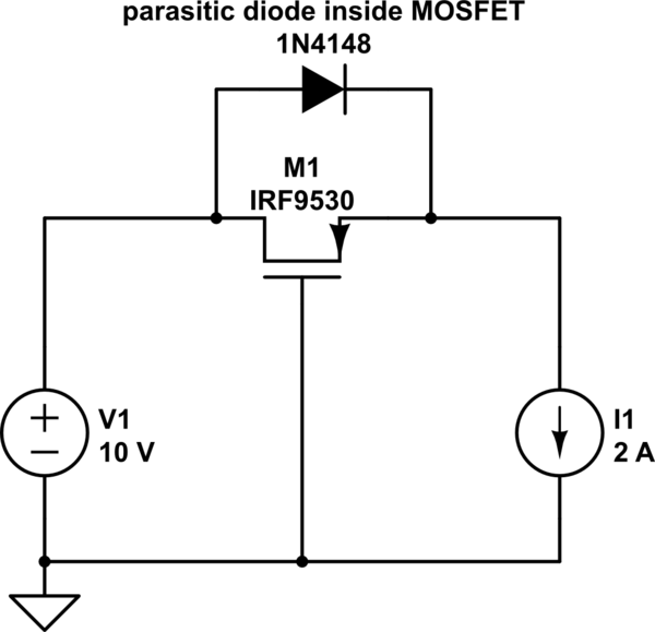
I read somewhere that this can be used for the reverse polarity protection in the circuit. But I am quite confused with its operation. Can somebody help me with this.

simulate this circuit – Schematic created using CircuitLab
I read somewhere that this can be used for the reverse polarity protection in the circuit. But I am quite confused with its operation. Can somebody help me with this.

simulate this circuit – Schematic created using CircuitLab
This is a very handy reverse polarity protection scheme.
A P channel MOSFET turns on when \$V_{gs}\$ is negative, probably starting around -3V to -5V. When power is switched on, \$V_{gs}=0V\$. This is where the parasitic diode drawn across the MOSFET in the datasheet comes into play (drawn for explanation purposes only, do not put a diode between the drain and source). It allows current to flow, drain to source, and drops about 1V.

simulate this circuit – Schematic created using CircuitLab
Assuming a supply voltage of 10V:
$$V_{gs}=V_g-V_s=0V-9V=-9V$$
The MOSFET is driven into saturation. Since the MOSFET's on resistance, \$R_{ds(on)}\$, is around \$25m\Omega\$, the parasitic diode gets shorted.
If the polarity is reversed, the parasitic diode never conducts, thus never allowing the MOSFET to turn on.
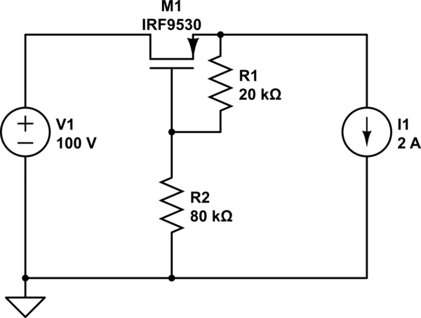
You need to be mindful of the maximum \$V_{gs}\$ in the datasheet. The MOSFET may be able to switch 100V, but the maximum \$V_{gs}\$ may only be 20V. In that case, you must put some kind of voltage divider in place to protect the gate of the MOSFET:
