0
\$\begingroup\$

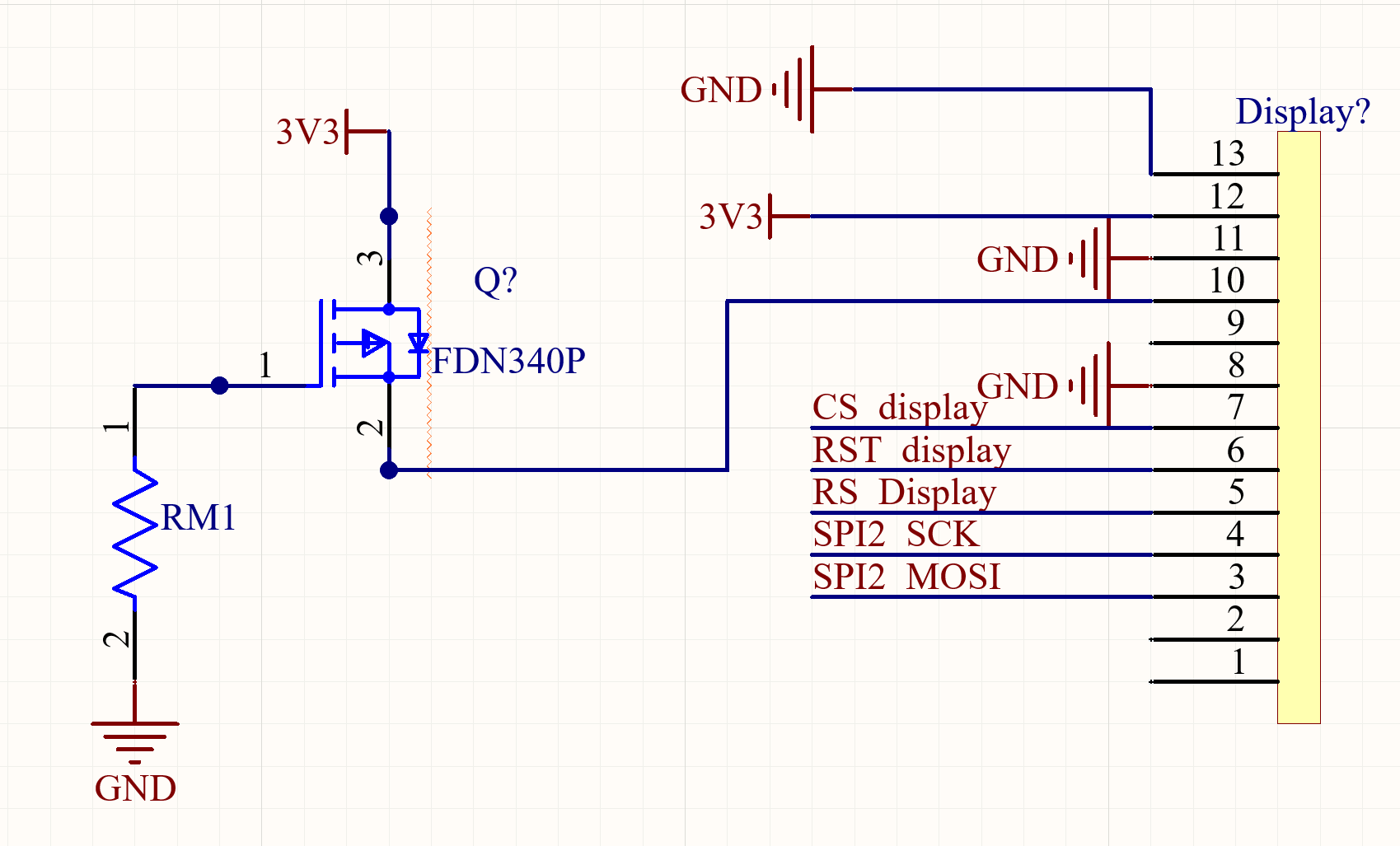
I have created a PCB with a microcontroller (3.3V logic) and a 1.14-inch TFT display.

The circuit I have right now powers the display, and it works great with the PCB I ordered!

Current design

However, I now need to be able to control the power supply to the display using the microcontroller. Currently, it's taking its power directly from the battery. Here's what I want:

Pin 12 of the display: Controlled by an output pin of the microcontroller. When there's 0 V at the output pin, pin 12 should not be able to draw any current, hence it should be an open circuit. When there's 3.3V at the output pin of the microcontroller, I want pin 12 to act just like in the circuit above, with a connection to the 3.3V (power supply battery).

The same goes for pin 10 of the display: Controlled by another output pin of the microcontroller. When there's 0 V at the output pin, pin 10 should not be able to draw any current, hence it should be an open circuit. When there's 3.3V at the output pin of the microcontroller, I want pin 10 to act just like in the circuit above, with a connection to the 3.3V (power supply battery).

The purpose of this is to completely shut down the display to ensure it does not draw any current. When 0 V is at the output pins of the microcontroller, the microcontroller is in sleep mode, and it should be able to remain like that for a month without the display or transistor drawing any current.

How should I solve this? I see there are solutions using both bipolar transistors and MOSFETs. What is the best solution in my case? Is there perhaps any other way to make this work?

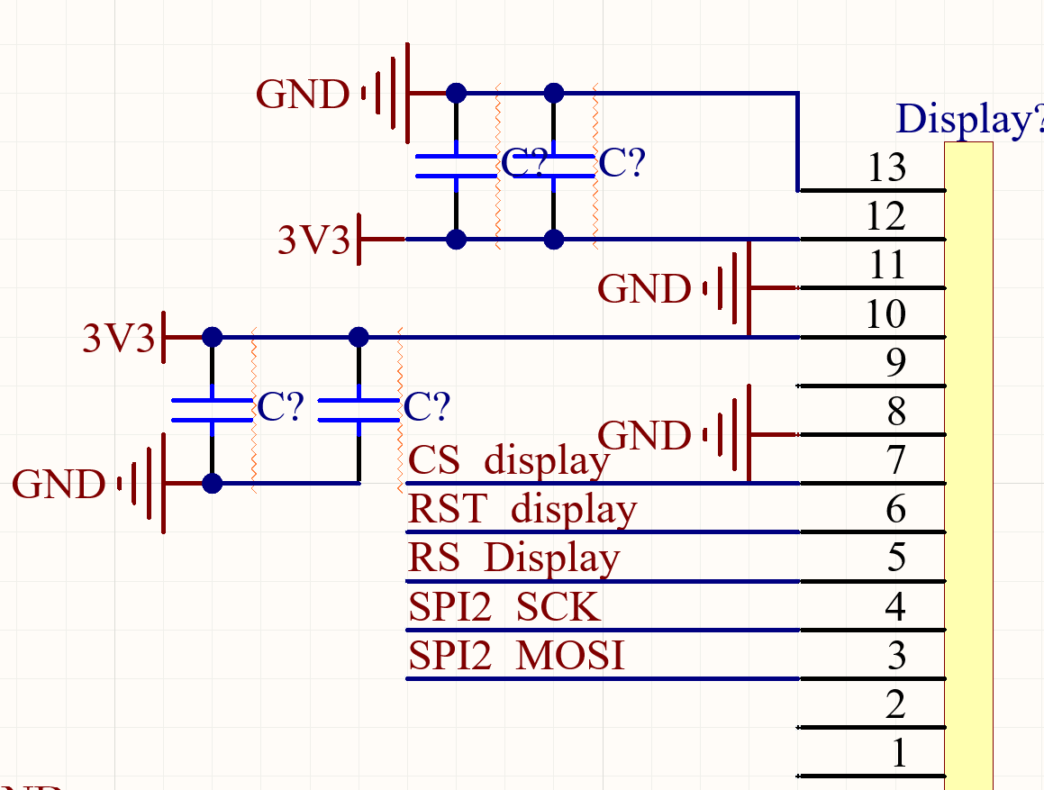
Could this be a solution to my problem? (And of course to the same thing with PIN 12). The gate will be connected to the microcontroller output.

enter image description here

\$\endgroup\$
7
  • 1
    \$\begingroup\$ Easiest solution: use a P-CH MOSFET and invert the command state (low = on). Remember to deassert or set low all the bus signals, so the display isn't powered through input clamp diodes. \$\endgroup\$ Commented Apr 15, 2023 at 19:35
  • \$\begingroup\$ @TimWilliams Isn't P MOSFET used for more high current applications? How would I invert the command state. And what do you mean with deassert bus signals? \$\endgroup\$
    – Gripen
    Commented Apr 15, 2023 at 19:40
  • 3
    \$\begingroup\$ @TimWilliams - Hi, I appreciate you're trying to help but please try to avoid answering questions in comments - that is not an allowed use of comments (see here and here). Using comments in this way can discourage others from actually answering, as the OP already has their "answer" in the comment so the time spent on writing a real answer can be seen as a waste. Comments also can't be edited or downvoted, so they bypass the full quality control and updating that is possible with real answers. Thanks. \$\endgroup\$
    – SamGibson
    Commented Apr 15, 2023 at 19:50
  • \$\begingroup\$ @SamGibson In this case, I'm at least partially answering the question to introduce the OP to additional information they likely weren't aware of (which is now confirmed). Once an answer is clear, I compose it (or someone else can "snipe" it, which, heck, saves me the trouble). This method avoids pitfalls like X-Y problems, that so frequently show up. (Or is it preferable to submit answers early and often, regardless of quality of question or answer?) \$\endgroup\$ Commented Apr 15, 2023 at 21:59
  • \$\begingroup\$ @Gripen PMOS and NMOS are available in a plethora of ratings, from the tiniest signals inside ICs themselves, to massive power transistors. There is something suitable for every application. You asked for "0V at the output pin" = display off; simply set 3.3V for off and 0V for on, instead. "Deassert" = set high-Z / undriven; if this is still confusing, perhaps you can show your schematic and source code, and we can show how to modify them? \$\endgroup\$ Commented Apr 15, 2023 at 22:02

1 Answer 1

2
\$\begingroup\$

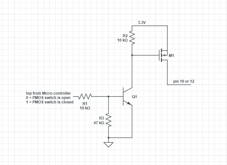
Here's the simplest I can think of for your requirement

enter image description here

For the PMOS, you need to use a 3.3V logic FET with the current rating that you need.

Note that when the PMOS is ON, there will be an extra current consumption through both the 10k resistors. I hope that is acceptable for your application.

EDIT: Note that the source and drain connections of the PMOS are to be done as shown in the diagram so that the bulk diode is reverse biased always.

\$\endgroup\$
11
  • \$\begingroup\$ I edited my question and added a circuit at the end. Could that one be a possible simple solution? \$\endgroup\$
    – Gripen
    Commented Apr 16, 2023 at 15:55
  • \$\begingroup\$ @Gripen No because you are using N-FET incorrectly. \$\endgroup\$
    – Justme
    Commented Apr 16, 2023 at 15:57
  • \$\begingroup\$ @Justme Why would that not work? Is there another way to get that simple circuit? \$\endgroup\$
    – Gripen
    Commented Apr 16, 2023 at 15:58
  • \$\begingroup\$ @Gripen Because a P-FET is correct solution for high side switching. N-FET as a high side switch will not get you 3.3V to load as you would need more than 3.3V at gate to have 3.3V on source. \$\endgroup\$
    – Justme
    Commented Apr 16, 2023 at 16:04
  • \$\begingroup\$ @Justme Okay, so using a P-MOSFET instead of an N-MOSFET in that exact circuit should work? I updated the Question with the new circuit. \$\endgroup\$
    – Gripen
    Commented Apr 16, 2023 at 16:13

Your Answer

By clicking “Post Your Answer”, you agree to our terms of service and acknowledge you have read our privacy policy.

Not the answer you're looking for? Browse other questions tagged or ask your own question.