10
\$\begingroup\$

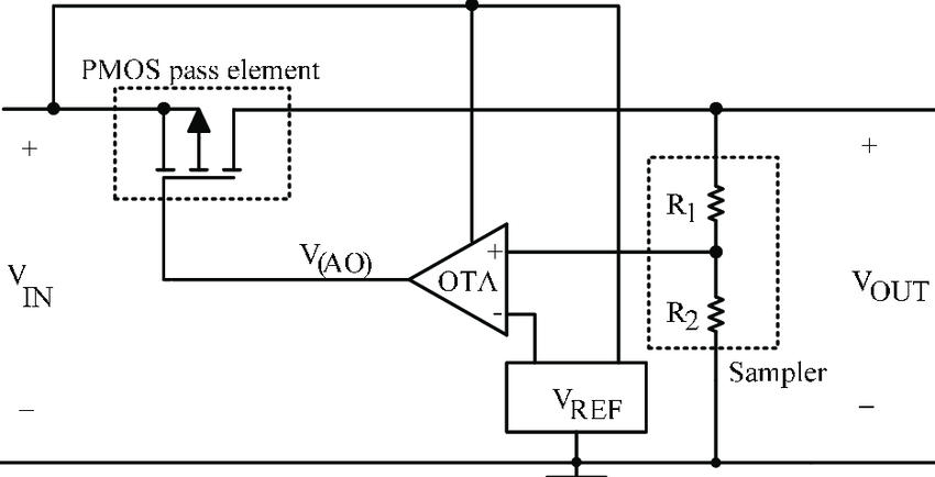
Looking over LDO / voltage regulator topologies I keep seeing examples of LDOs where the feedback network is connected to the non-inverting input terminal of the error amplifier.

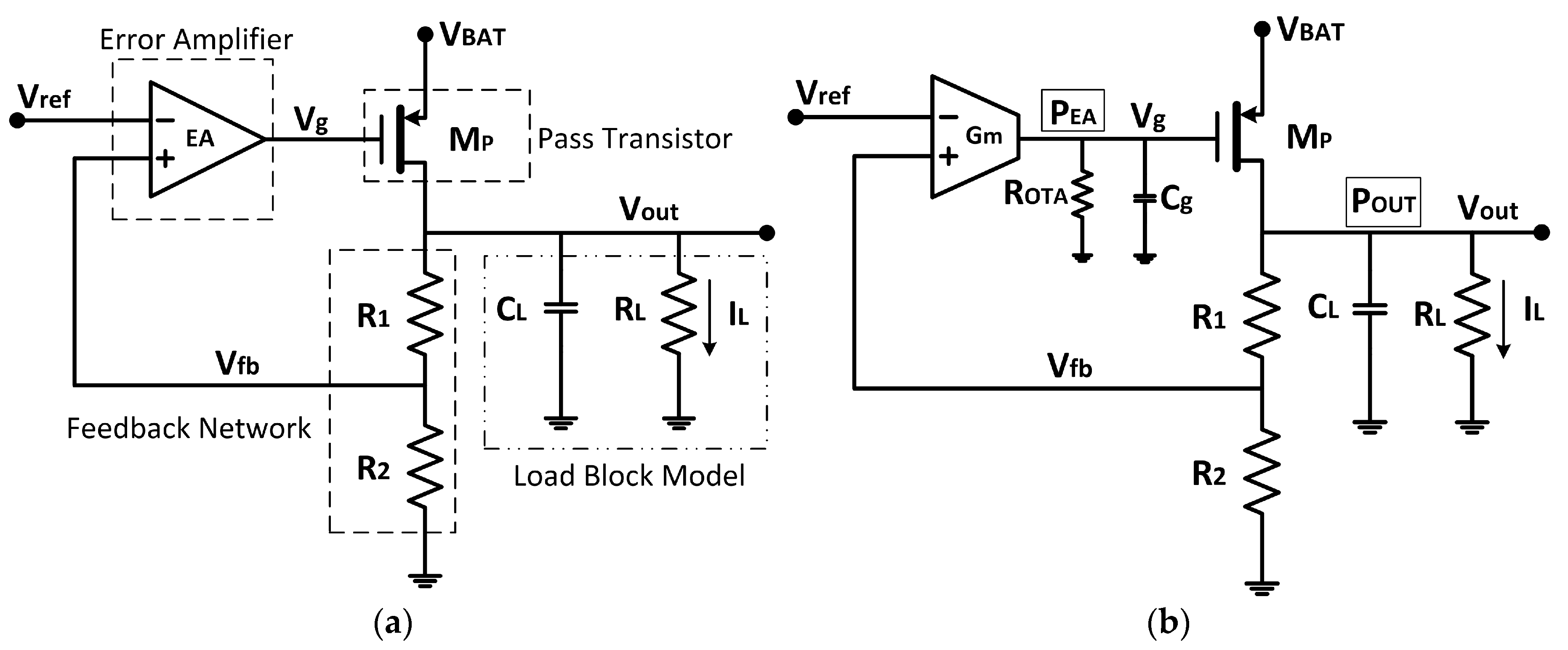
Like this: enter image description here

Taken from here.

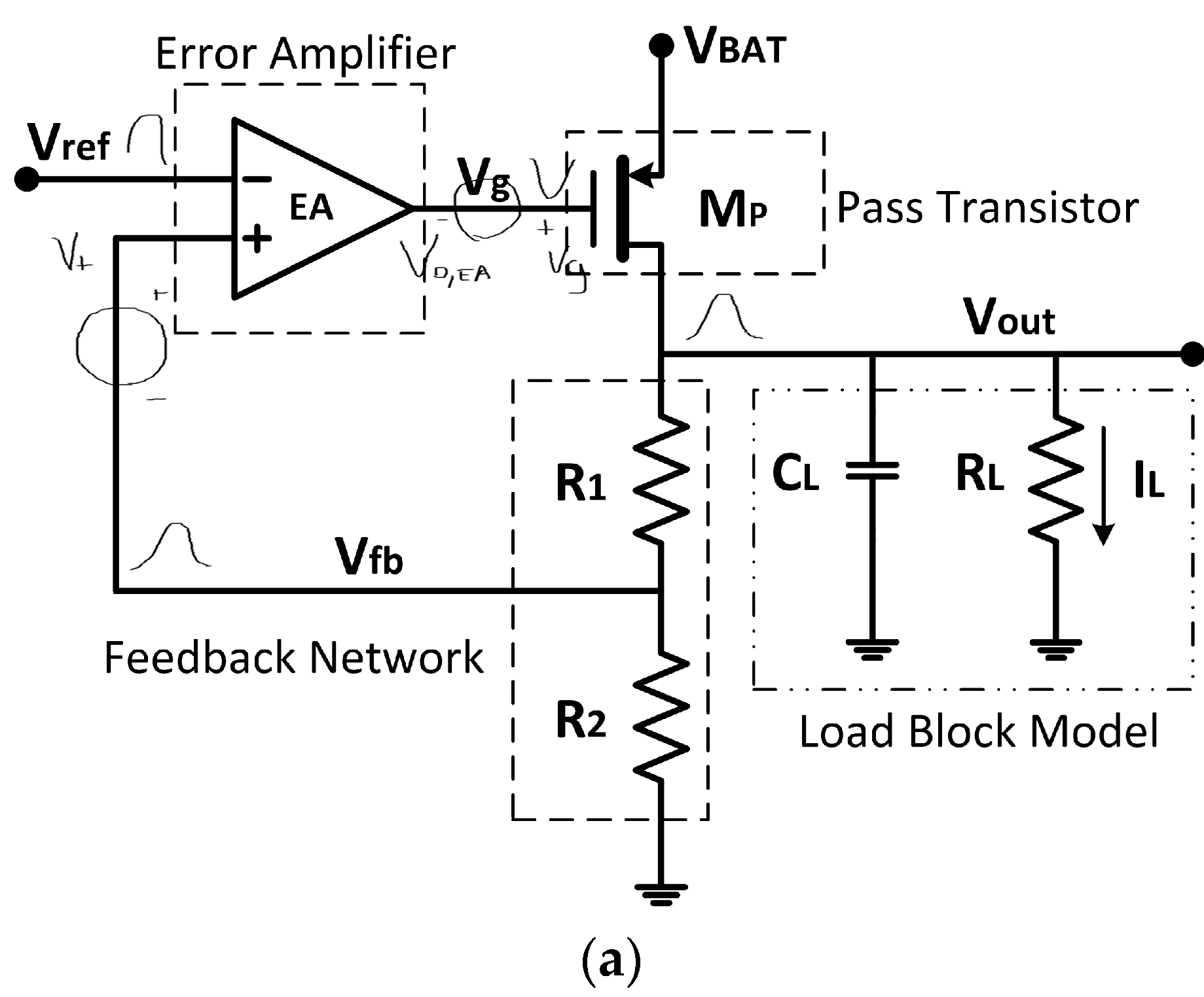
Or like this: enter image description here

Taken from here.

I found examples with the expected connection between the inverting input and output, but I am left to wonder how the circuits from above make sense.

Is this an example of positive feedback, an unknown to me circuit notation convention or something else?

\$\endgroup\$
3
  • 1
    \$\begingroup\$ Take a look here electronics.stackexchange.com/questions/351139/… at The Negative feedback vs Positive feedback at "DC". \$\endgroup\$
    – G36
    Commented Nov 3, 2023 at 10:58
  • \$\begingroup\$ @G36 I've taken a look and the images do paint a vivid picture. \$\endgroup\$ Commented Nov 3, 2023 at 12:55
  • \$\begingroup\$ Consider the result if the external transistor and prior components were instead included inside the op amp. What you get is the phase of the opamp inverting and the inverting and non-inverting inputs are effectively swapped. That should remove the apparent confusion. \$\endgroup\$
    – Russell McMahon
    Commented Nov 8, 2023 at 13:16

3 Answers 3

13
\$\begingroup\$

You must consider the whole feedback, not just the error amplifier but also the transistor. It is the transistor that adds a 180° shift, which changes positive feedback into negative.

\$\endgroup\$
11
  • 1
    \$\begingroup\$ The simple idea here is that a P-channel (pass transistor) is enabled with a low signal, and disabled with a high signal. So when the feedback system sees the output voltage rising above the reference the comparator goes positive and the pass transistor is switched off. So the output voltage is regulated at the Vref voltage \$\endgroup\$
    – Nedd
    Commented Nov 3, 2023 at 7:19
  • \$\begingroup\$ So this is a comparator that has in its feedback loop an inverting amplifier? \$\endgroup\$ Commented Nov 3, 2023 at 7:45
  • 1
    \$\begingroup\$ To better clarify the initial comment, the output voltage is actually regulated by the sample divider and the Vref voltage. \$\endgroup\$
    – Nedd
    Commented Nov 3, 2023 at 7:56
  • 1
    \$\begingroup\$ @nanofarad "robust to nonzero input currents crossing the loop break point". Forgive me, but what does this mean? \$\endgroup\$ Commented Nov 3, 2023 at 14:34
  • 1
    \$\begingroup\$ @Virgil_Tibbs In any feedback system, no matter where you choose to break the loop, you have both voltage and a current participating in that feedback. Many analyses will ignore one or the other, because they rely on you breaking the loop just before or just after a near-ideal device that lets you safely ignore it. An explicit example: If you broke the feedback loop in the middle of the voltage divider and used an analysis that ignored currents across the loop-break, you'd get nonsense answers. If your analysis does handle those currents, the math might be clunky but the answer will be right \$\endgroup\$
    – nanofarad
    Commented Nov 3, 2023 at 14:37
7
\$\begingroup\$

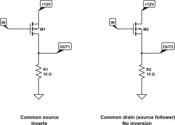
These two circuits look very similar, but the one on the left inverts, and the one on the right does not invert:
schematic

simulate this circuit – Schematic created using CircuitLab

On the left is a "common source" setup, using a P-channel MOSFET, whose output (taken at the drain) is inverted with respect to the input at the gate. That is, as IN rises in potential, OUT1 falls, and vice versa.

On the right we have a common drain configuration, otherwise known as a "source-follower", employing a N-channel MOSFET. The word "follower" in the name suggests that the MOSFET's source (the output here) "follows" the input at the gate, implying that there's no inversion. In other words, a rise in potential at IN will result in a rise at OUT2. Conversely, if IN decreases, so does OUT2.

I explain this distinction in much greater detail in this answer.

The same difference in behaviour can be observed in bipolar transistor circuits, where inversion occurs in the "common emitter" arrangement, but not in "common collector" (also called "emitter follower"). The distinction is in where you derive the output signal. For the common emitter circuit, the output is the collector, and is inverted with respect to the signal input at the base, whereas the the emitter-follower does not invert:
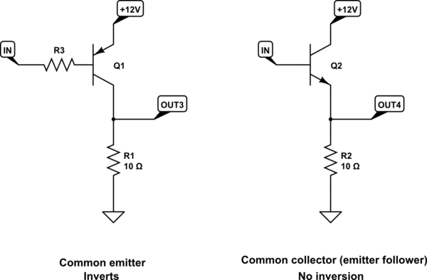
schematic

simulate this circuit

You'll notice that in all those circuits where you identified feedback returning to the non-inverting input, which seems to contradict how we usually implement negative feedback using the inverting input, feedback is derived from the drain of the transistor stage, which implies there's an inversion from that stage. They all use "common source" stages.

To obtain negative feedback, the goal is to have the op-amp output change in a manner that decreases the overall output, as that output rises. That is, the op-amp must oppose any change in overall output. If feedback were taken directly from the op-amp's own output, then that feedback must be applied to the op-amp's inverting input, so that a rise in output would result in the op-amp opposing that very rise, and vice versa.

However, in these circuits, due to the inverting action of the transistor stage, the overall output actually rises as the op-amp's output falls (and vice versa), and so to produce negative feedback that overall output must be coupled back to the op-amp's non-inverting input instead.

If there's an inverted relationship between op-amp output and overall output, which happens in all these examples due to the inverting transistor stage, then you must also reverse the op-amp's behaviour, by applying feedback to the non-inverting input instead. Otherwise feedback would be positive, in which a slight rise (or fall) of overall output would result in a further rise (or fall) in overall output, causing a much larger rise (or fall), and so on, running off to some extreme.

If you inserted another inverting stage (using an additional transistor or op-amp) between the existing op-amp and transistor stages, then you could once again apply feedback to the inverting input, as you would in classic amplifier designs. That's because the overall output, and the op-amp's output would once again be back "in phase".

If you replaced the common-source transistor stage with a common-drain stage instead, then again there would be no inverted relationship between op-amp and overall output, and you would also apply feedback (as usual) to the op-amp's inverting input.

Here are some stable systems successfully employing negative feedback. Note the number of inverting stages in the path between op-amp output and overall output, and see how an odd number of inversions requires feedback to be applied to the non-inverting input:
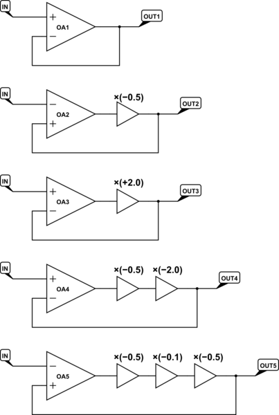
schematic

simulate this circuit

In both circuits below we successfully employ negative feedback, but the difference between them is really subtle:
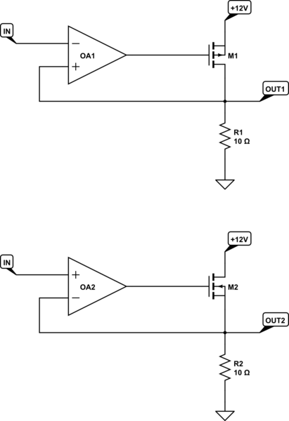
schematic

simulate this circuit

Hopefully you noticed that the bottom transistor is configured as a source follower, which does not invert, and therefore feedback is applied to the inverting input, as usual. However, the top transistor is common source, that feedback signal is inverted with respect to the op-amp's own output, and overall output must be fed back to the non-inverting input for that feedback to be negative.

\$\endgroup\$
3
  • \$\begingroup\$ That's really nice. Beautiful answer. In the image with multiple amplifiers one after another, the whole chain is part of the feedback loop, right? To test the loop gain of the equivalent I only need to break the loop between any two of those amplifiers, right? \$\endgroup\$ Commented Nov 3, 2023 at 14:03
  • \$\begingroup\$ @Virgil_Tibbs That's right, break the chain anywhere, and measure the relationship between the severed input and output to reveal if feedback is negative. \$\endgroup\$ Commented Nov 3, 2023 at 14:06
  • \$\begingroup\$ @Virgil_Tibbs and of course reveal the loop gain. \$\endgroup\$ Commented Nov 3, 2023 at 14:19
7
\$\begingroup\$

There's no positive feedback here. The output device is a PMOS, and thus, it is connected to the (+) input terminal to keep the loop negative.

To understand this better, on your left circuit (a).

  1. Upward swing on \$V_{ref}\$ and constant voltage at (+) causes \$V_g\$ to go down (it's an small signal comparator).
  2. \$V_g\$ going down causes Mp's drain (\$V_{out}\$) to go up. Signal inversion.
  3. If \$V_{out}\$ goes down, so does \$V_{fb}\$, but by a factor of \$\frac{R2}{R2+R1}\$ lower in magnitude (i.e. equal to \$V_{ref}\$).
  4. Thus, \$V_{fb}\$ has the same upward as \$V_{ref}\$. Therefore, V(+)-V(-)=0, thus we keep the error signal equal to 0, which is the whole point of a feedback system (In this case, for simplicity, assuming EA has infinite gain).

Follow the signal chain; there's no positive feedback.

EDIT:

About your question where to break the loop. It doesn't matter where you break it, because you are still in the loop. However, it matters what kind of source you use to excite the loop and compute the return.

And, actually, it's better not to break the loop, but instead insert a voltage or a current source such that the biasing is kept intact. This is useful for simulation, in particular.

In this loop (the amplifier on the left), we have 2 nodes where the right-hand impedance is high and the left-hand is low. Namely, \$V_{fb}\$ and \$V_g\$.

You can insert a series voltage with an AC amplitude of 1 (and DC = 0V) separating \$V_{fb}\$ from the (+) input of the op-amp. Then, in your simulator, you can simply plot \$\frac{V_{fb}}{V(+)}\$ (remember, you have to go around the loop, so you start from V+ and end in \$V_{fb}\$, which would your "output").

Likewise, you could also insert a voltage source in series with \$V_g\$, thus separating the op-amp output node and the PMOS gate. Thus, you can simply plot \$\frac{V_{o,EA}}{V_g}\$.

In any of those situations, the low-frequency loop gain would be equal to \$A_v g_{m,Mp} \frac{r_{o,Mp}R_2}{r_{o,Mp}+R_2+R_1}\$, assuming \$A_v\$ is the open-loop gain voltage of the op-amp, and the low-frequency signal model of the PMOS is just a \$g_{m,Mp}\$ with an output impedance \$r_{o,Mp}\$... and ignoring the load impedance.

If you'd do it at the drain of the PMOS, it'd be complicated because it's difficult to tell whether the impedance looking from at the drain of the PMOS is a lot higher than the feedback resistance, maybe it is. Same complication at the junction between \$R_1\$ and \$R_2\$.

To overcome this complication, Middlebrook came up with this method, where he uses the loop gain calculated from a voltage and a current source. He combines both results to produce a loop gain, and you don't have to care where you put these 2 sources. The only shortcoming of this method is that it doesn't account for reverse transmission, only for a forward transmission. But anyhow, it's still quite a good approximation to the true result for most electronic feedback systems.

PMOS LDO

\$\endgroup\$
6
  • \$\begingroup\$ Well I got to admit that I was working from the assumption that negative feedback meant a direct connection between the output and the inverting input. \$\endgroup\$ Commented Nov 3, 2023 at 7:18
  • \$\begingroup\$ You have to follow the inversions in the signal chain. In this case, voltage amplification means series feedback at the input: there has to be a subtraction between 2 input voltages. If vref swings up, for negative feedback to function properly, voltage at (+) terminal must be also be swinging up. If you find a contradiction to that, there's no negative feedback. \$\endgroup\$
    – Designalog
    Commented Nov 3, 2023 at 7:20
  • \$\begingroup\$ This is confusing. I know that in order for the feedback to be negative the loop gain should be negative. Is this applicable here, as well? Where do you break the loop, at the drain of pass transistor? And you input a test voltage at the upper end of R1? \$\endgroup\$ Commented Nov 3, 2023 at 7:37
  • \$\begingroup\$ @Virgil_Tibbs Think of it as simple non-inverting voltage amplifier. There, you also have both input terminals swinging in the same direction such that the error signal equals 0. To know that the feedback is negative, you can simply do the mental exercise that there's a voltage disturbance in any node (voltages goes either up or down, you can choose arbitrarily). Then, once you follow the loop, the conclusion must be that loop suppresses this voltage swing (at least it works for this kind of feedback topology). \$\endgroup\$
    – Designalog
    Commented Nov 3, 2023 at 7:51
  • \$\begingroup\$ If you have more questions, check out my profile to reach me. \$\endgroup\$
    – Designalog
    Commented Nov 3, 2023 at 7:54

Your Answer

By clicking “Post Your Answer”, you agree to our terms of service and acknowledge you have read our privacy policy.

Not the answer you're looking for? Browse other questions tagged or ask your own question.