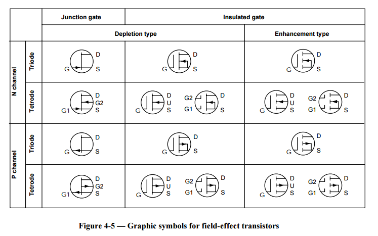
I've been on this site now a couple of months and I notice various symbols used for MOSFETs. What is the preferred symbol for an N Channel MOSFET and why?
-
\$\begingroup\$ I doubt you'll get an objective answer to this question, since there are multiple opinions on the matter and (to my knowledge) no international standards on component symbols. (The fact that you've seen multiple symbols here should be a hint that 'anything goes'.) \$\endgroup\$– Adam LawrenceCommented May 14, 2013 at 21:04
-
\$\begingroup\$ You should use the symbol which is pertinent. If you're really making a point about an enhancement device your should really use one with a dotted channel - for example. But for the most part, it doesn't really matter. \$\endgroup\$– placeholderCommented May 14, 2013 at 21:08
-
\$\begingroup\$ chat.stackexchange.com/transcript/message/9424690#9424690 \$\endgroup\$– jippieCommented May 14, 2013 at 21:11
-
2\$\begingroup\$ There is an international standard for these symbols, whether anyone likes it or not. I'm guessing that many readers will not. See answer below. \$\endgroup\$– Joe HassCommented Dec 22, 2013 at 12:25
-
\$\begingroup\$ When in doubt pick the symbol used in the manufacturer's datasheet. \$\endgroup\$– Noah SpurrierCommented Sep 28, 2014 at 19:12
5 Answers
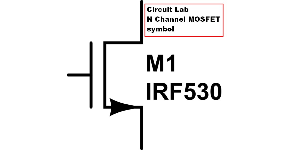
It is likely that you saw a Circuit Lab sysmbol and that this caused you to ask this question. The Circuit Lab N Channel MOSFET symbol is both unusual and illogical.
I'd avoid using them if at all possible.
Read on ...
Acceptable [tm] N Channel MOSFET symbol tends to have these characteristics.
Gate symbol on one side.
3 "contacts" on other side vertically.
Top of these is drain.
Bottom of these 3 is source.
Middle has an arrow pointing INTO the FET and the outside end is connected to source.
This indicates that there is a connected body diode and that it is non conducting when the source is more negative than the drain (arrow is same as would be for a discrete diode).
Any symbol which obeys these guidelines should be "clear enough" and OK to use.
I have very occasionally seen people use a symbol which does not comply with these guidelines but which is still recognisable as an N Channel MOSFET.
SO. Any of these are OK, and you can see the differences for the unmarked P Channels.

But!!!
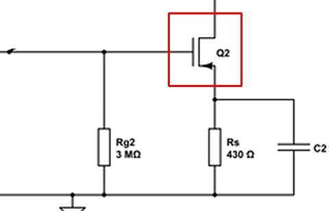
Jippie's example shows the rogue version.
[Note: See below - this is in fact intended to be a P Channel sysmbol].
Truly horrible. I'd have to wonder if this was a P Channel symbol or an N Channel one.
Even the discussion it is taken from has people expressing uncertainty re arrow direction. As shown IF that is an N Channel then it is implying body diode polarity and NOT current flow in source.
Thusly
________________'
Circuit Lab is apparently the (or a) culprit.
This is their symbol for an N Channel MOSFET.
A nasty piece of work, alas.
Arrow shows usual drain-source conduction direction BUT as a MOSFET is a 2 quadrant device and will provide a true resistive on channel with \$V_{gs}\$ positive BUT \$V_{ds}\$ negative, the arrow is meaningless and, as it is in the opposite direction to most N Channel MOSFET sysmbols it is misleading to most. (Note the proper use of this symbol in table below).
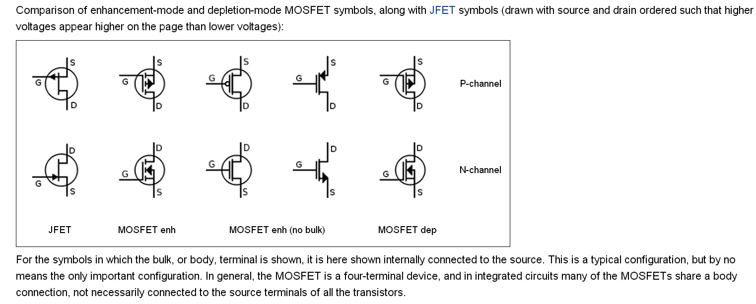
USER23909 helpfully pointed out this page - Wikipedia - MOSFET . This page includes the following symbols. User xxx says these may be IPC standards, but Wikipedia is silent re their source.
Wikipedia MOSFET symbols
-
1\$\begingroup\$ This is what I suspected - I don't mind a plethora of MOSFET symbols that are all takes on a similar theme but the Circuit_Lab symbol just seems to be in it's own league - it might be trying to mimic a BJT - the emitter and source (for NPN and N channel) do point the same way (now that I have become semi-accustomed to the symbol). Is this the way forward for generic enhancement mode FETs or should it be frowned upon? \$\endgroup\$– Andy akaCommented May 15, 2013 at 11:49
-
\$\begingroup\$ @Andyaka Look at the Wikipedia symbols at the bottom of my answer and at Kurt's comments. The two leads with arrow on source versions are MOSFETS wity no body diode. I think Silicon on Saphire gives you that as of right and you can do it with silicon with due design care. \$\endgroup\$– Russell McMahon ♦Commented May 15, 2013 at 17:37
-
\$\begingroup\$ And note that you may on occasion come across a four terminal MOSFET, where the substrate terminal is explicitly broken out. \$\endgroup\$ Commented Dec 22, 2013 at 2:43
-
5\$\begingroup\$ The Circuit Lab symbol is logical and standard, but not the preferred symbol for discrete MOSFETs. It's the symbol used to diagram IC internal circuitry. The cause of the confusion is due to the natural assumption that the arrows represent the same thing. They don't. In one version the arrow is on the substrate Bulk connection. In the other version the arrow is on the Source connection. If you think about the way current flows in a MOSFET then the arrow direction is logical depending on which connection it is show on. Yes, it's a confusing, stupid standard to have established, but logical. \$\endgroup\$ Commented Sep 28, 2014 at 19:27
Yes, Virginia, there is an accepted, published international standard for these symbols. It is IEEE Standard 315/ANSI Y32.2/CSA Z99 and it is mandatory for the US DoD. The standard is intended to be compatible with approved recommendations of the International Electrotechnical Commission. The standard is very detailed and lengthy so I'll show just a few examples.
This is an enhancement-mode, four-terminal, NMOS transistor. Note that the gate terminal shall be drawn as an L-shape with the corner in the L adjacent to the preferred-source terminal. The arrowhead pointing inward at the bulk/body terminal indicates that the body is P-type (and so the source and drain are N-type). The vertical line segments for the drain, bulk, and source connections are disconnected to show that the transistor is an enhancement-mode device.

Here is the same symbol, except for a depletion-mode transistor. Note that the vertical segments for the drain, bulk, and source are continuous.

The standard allows for an internal connection between the source and bulk, as shown in this depletion-mode NMOS.

-
1\$\begingroup\$ In practice IEEE is more US than international. I'd be interested to find out if these have trickled into some IEC standard. IEC has some joint committees with ANSI, so they might have. IEC 60617 is probably where they are. \$\endgroup\$ Commented Jan 1, 2015 at 19:57
As stated, there really is no accepted standard. This is partly because there are so many different kinds of FETs and partly because people mix them up with BJTs (such as the arrow direction.)
If you are using a specific part and the datasheet from the manufacturer shows a specific circuit symbol, then use that symbol! Many people will argue that it doesn't really matter, but that is nonsense. If a circuit designer picks a particular type of component, then that component should be represented appropriately in the schematics. Each type works differently. Saying that the circuit symbol doesn't matter is essentially saying that the type of part doesn't matter either.
I have had to create my own Eagle library with various parts to represent different kinds of FETs:
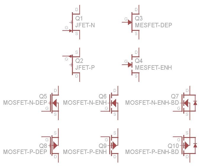
These includes JFETS, MESFETS, and MOSFETs in depletion mode, enhancement mode, and enhancement bode with a body diode. Notice the location of the gate relative to the body for P and N channels, the solid line for depletion mode, the dotted line for enhancement mode, and the additional body diode.
However, there are still many other types of MOSFETs that could be represented differently, such as those with dual gates or showing the body (substrate) connection when it is not shorted to the source. Drawing the circle around the FET is also common, but I have chose not to do it here because it clutters up the schematic and makes the component values difficult to read. Occasionally, you will see the arrow pointing in the opposite direction at the source - this typically means enhancement mode with no bulk.
-
1\$\begingroup\$ Why do you have zener bars on the body diodes for the ENH-BD devices? \$\endgroup\$ Commented Dec 31, 2016 at 5:04
-
\$\begingroup\$ Good catch. That particular part used Schottky diodes, and I can only imagine it was a rendering error when I made the image. Although, realistically, it shouldn't have any bars at all for most body diodes. I'll fix that when I have a minute... \$\endgroup\$ Commented Jan 3, 2017 at 0:00
Here's the relevant page from CEI EN 60617-5:1997, which is basically the Italian incorporation of the IEC 60617 standard. Other than the fact that they call MOSFETs IGFETs, it's basically using the same symbols as the IEEE standard, but sans circles.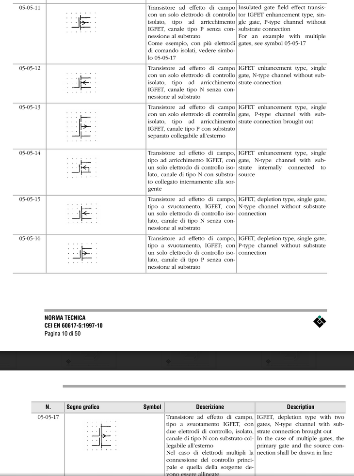
Note that the dot grid is not part of the symbols. It's only used in this standard to indicate how big the symbols are to be drawn relative to other symbols in the standard.
The (common) p-channel MOSFET with substrate internally connected doesn't appear to have a symbol in this version of the standard, i.e. the standard is lacking a p-channel version of symbol 05-05-14. As stefanct points out in a comment below, this list is just a list of examples of how standard's elements are to be combined, so the non-listed variants are composed by analogous rules.
By the way, JEDEC also has a standard for these symbols in their JESD77:
-
\$\begingroup\$ Re. IEC: the pages you cite are listing examples only. The standard defines various elements of a symbol that can be combined to form different components. In the case of transistor elements these are 05-01-01 to 05-01-24 (diodes follow as 05-02-01 to 05-02-05). \$\endgroup\$– stefanctCommented Apr 18, 2017 at 20:50
-
\$\begingroup\$ @stefanct: Ok, that makes most sense from the possibilities I imagined/enumerated in my answer. \$\endgroup\$ Commented Apr 19, 2017 at 23:34
Some MOSFETs, including most that are in "standalone" packages, have the source connected to the drain. Such MOSFETs will have an inherent diode in them between the source and drain, which will conduct if the MOSFET is biased in the direction opposite the direction it would typically switch (e.g. if souce is more positive than drain for an NFET, or more negative than drain for a PFET). The arrow on the symbol indicates the polarity of this diode.
Other MOSFETs, especially those within digital logic chips, have the substrates connected to a power rail, independent of their source, drain, and gate connections. While one could include such connections on a schematic, doing so would be somewhat like adding power-rail connections to every single logic gate on a schematic. Since 99% of logic gates have their VDD tied to a common VDD, and their VSS wired to a common VSS, such connections would be visual noise. Likewise when 99% of NFETs have their substrate tied to the most negative point and 99% of PFETs have their substrate tied to the most positive point. If the substrate connection of a MOSFET is implied rather than shown, one could distinguish between NFETs and PFETs by using an arrow for the unconnected substrate terminal, but that could be somewhat odd.
Further, while it is possible to construct a MOSFET whose source-drain channel is symmetric, using an asymmetric channel will improve performance when the device is used to switch current in one direction, at the expense of its performance in the other direction. Since this is often desirable, it is often helpful to have schematic symbols which distinguish between the source and the drain. Since the source-connected substrate symbol "marks" the source lead, and since BJT symbols mark the emitter whose use most resembles the source, it is common for MOSFET symbols which don't have a marked substrate to use an arrow whose direction is analogous to that of a BJT.
To my mind, the way to appreciate the distinction is to realize that when an arrow is shown for the substrate, that represents a place that one must generally prevent current from flowing in the direction of the arrow, whereas when an arrow is shown for the source, that represents the desired current flow.
My own preference is to use an NFET symbol with an outward-pointing arrow on the source, possibly with a back-biased source-drain arrow in cases where that would be relevant. For a PFET, I use an inward-pointing source arrow, and also add a circle on the gate. When I am sketching out conceptual VLSI designs for illustrative purposes (I've never been involved in the design of an actual fabricated chip) the NFET symbol and FET symbol for transistors used as bidirectional pass-gates won't have any arrow, but will use the circle or lack thereof as a polarity indicator.
Incidentally, I find it curious that in cases where discrete MOSFETs are used to produce pass-gates, it's typical to use two back-to-back FETs, each of whose source is tied to the substrate. I can understand that in cases where a circuit would tie a MOSFET's source to its substrate, manufacturing a part with them connected is cheaper and easier than including an insulator; I would think, though, that it should be cheaper to make one MOSFET with an isolated substrate than to make two MOSFETs each with a source-substrate connection. I wonder if individual source-substrate connections would be generally "preferred" within a VLSI design except for the fact that it's easier to connect many transistors with a common substrate than to isolate the substrate connections of transistors which have isolated sources. Perhaps the situation is somewhat analogous to vacuum tubes (some tubes connect the cathode to one of the filament connections, but others use a separate cathode pin)?

