Can a solder mask on a PCB reduce a magnetic field emitted from traces where an AC current is applied? If not, what could I do to minimalize this magnetic field emitted from a PCB? Because I know that if a trace emits a magnetic field, this field then induces on the other trace and an induced voltage is created. And this voltage is unwanted.
-
1\$\begingroup\$ Magnetic coupling is avoided by good PCB layout and control of rise times since shielding is very difficult and not very effective. If you're having issues with coupling, look at your layout. \$\endgroup\$– user1850479Commented Jan 5 at 0:45
3 Answers
No, it will not. Magnetic fields are only attenuated slightly in the low frequency range by most materials and soldermask. In the high frequency range in the GHz the dissipation factor comes in to play.
There are no materials that operate in normal temperatures that can block magnetic fields, only attenuation is possible. Mumetal being one of the leading materials.
The best way to lessen the impact of magnetic fields is to place traces away from each other.
The effect is called mutual inductance coupling, it is similar to a transformer in the circiut world. Since it is magnetic, the coupling only occurs when the magnetic field is changing. You can calculate/estimate the coupling with electromagnetic equations.
Solder mask is a dielectric so it does mostly nothing to magnetic fields.
A way to prevent magnetic emission from a PCB trace where current circulates is to have the return current path very close to the trace. This way the fields emitted by the trace and the return path are almost identical but opposite polarity and cancel.
This can be achieved either by
Running trace and return side by side and very close (as in differential pairs)
Having the trace on top of a ground plane, in this case the return current will follow the path of minimum impedance. If frequency is high enough, inductance dominates, so the minimum impedance return path is right under the trace, which also results in minimum emissions.
Can a solder mask on a PCB reduce a magnetic field emitted from traces where an AC current is applied?
It will have no benefit at all.
If not, what could I do to minimalize this magnetic field emitted from a PCB?
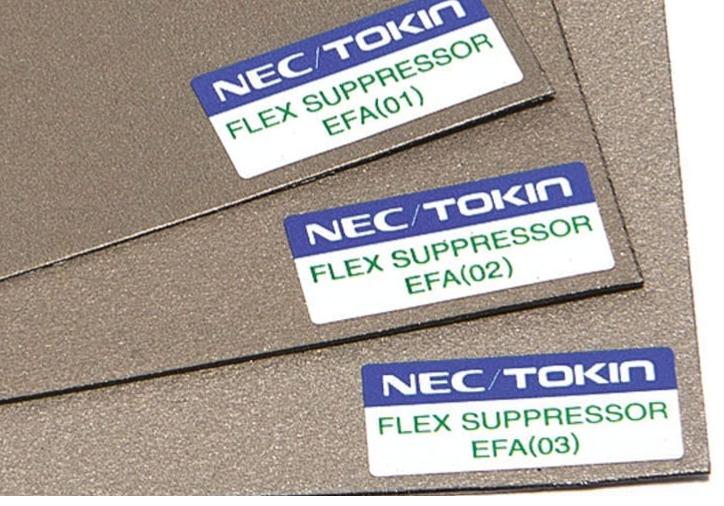
Prevention is better than cure so, if you can't arrange the return path of current to closely follow the forward path of current (cancelling the external magnetic field) then, consider using something like ferrite sheet/foil (a cure): -
Image taken from KEMET Polymer, Magnetic Flex Suppressor, 240mm x 240mm x 0.2mm. It can be cut to size and comes in various offerings of permeability suiting a broad range of applications. There are several suppliers of such material and, Kemet is just one of them.
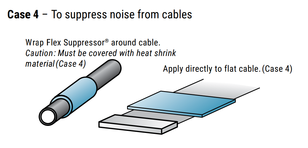
It works by providing a "short-cut" for lines of flux that would surround a current carrying an AC current. Example from datasheet: -
if a trace emits a magnetic field, this field then induces on the other trace and an induced voltage is created.
An induced voltage is only created when the magnetic field is changing.


