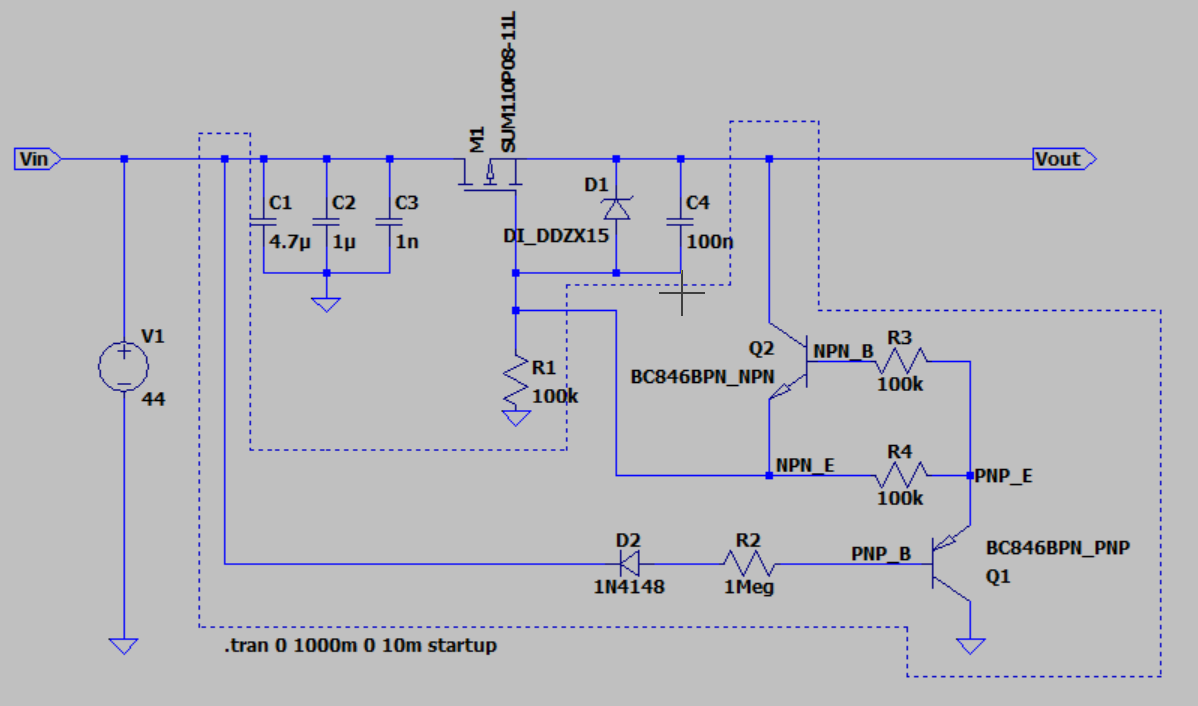
The below is a reverse polarity circuit with additional components around it. I would like to understand the exact functionality of the additional circuitry in dotted lines.
\$\begingroup\$
\$\endgroup\$
4
-
1\$\begingroup\$ Ravi Prasad - Hi, Re: "I came across the following reverse polarity circuit" Where did you come across it? To comply with the site rule on referencing, you should include a suitable citation for material copied or adapted and posted on Stack Exchange. For an online source, adding the webpage / PDF / video title & its link are the minimum; see the rule above for more details. Please edit your question to add a suitable reference. || Please see the tour & help center as the site rules differ from typical forums. TY \$\endgroup\$– SamGibson ♦Commented Jan 8 at 11:44
-
1\$\begingroup\$ Please double-check your source. It looks like Q2 should be PNP rather than NPN. As an NPN, there is no source for its base current. But as a PNP (emitter connected to Vout), it would actively clamp the gate of M1 in the off state as soon as Q1 turns on as a result of Vin becoming less than Vout. \$\endgroup\$– Dave TweedCommented Jan 8 at 12:42
-
\$\begingroup\$ Hi Dave, BC846BPN chip contains npn pnp transistors. Connections are same exactly shown circuit. \$\endgroup\$– Ravi PrasadCommented Jan 11 at 15:32
-
\$\begingroup\$ I understand that, but it still doesn't make sense to use a NPN in that position. \$\endgroup\$– Dave TweedCommented Jan 12 at 12:44
Add a comment
|

