1
\$\begingroup\$

This is a follow-up to a similar question I asked recently. Let's say I'm using an N-Channel MOSFET with Vds(Max) of 30v, Vgs(max) of +- 20v, and Vgs(th) of 2v. I want to use it as a high side switch, where the supply voltage is 24v and the signal voltage is 28v.

The drain of the MOSFET will be hooked up to 24v, and the source will be connected to the positive side of the load and the negative side of the load will be connected to ground.

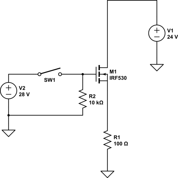
schematic

simulate this circuit – Schematic created using CircuitLab

When the signal is at 28v, the load should be on, and the Vgs is 4v, which works as expected. Now, let's look at the situation where the load is off. Using the same way Vgs(on) was calculated, Vgs(off) becomes -24v! This is outside the max range of the MOSFET. However, Vgs(on) is calculated under the assumption that the MOSFET is already on and the 24v is already present at the source. But isn't this just a theoretical for calculations? Is the -24v of the Vgs(off) really -24v and outside the range of the MOSFET?

\$\endgroup\$
6
  • \$\begingroup\$ You haven't told us enough about your circuit for us to know what voltage will be on the source, so there's no way for us to answer this. \$\endgroup\$
    – The Photon
    Commented May 24 at 16:25
  • \$\begingroup\$ Described situation cant happen. You assume that potential on gate does not change. And therefore MOSFET stays open :) In other words, you have to change Vgs first and then transistor reacts by closing or opening. You cannot "magicaly" turn transistor OFF without any change on gate.... \$\endgroup\$ Commented May 24 at 16:30
  • 1
    \$\begingroup\$ Instead of describing the circuit, use the Circuit Lab schematic tool in the toolbar of the question editor. Many of us can read a diagram easier than the text. \$\endgroup\$
    – user319836
    Commented May 24 at 16:44
  • \$\begingroup\$ If the load can store charge and hold its own input at +24V, then yes, this is something you need to deal with. Normally, as the gate voltage falls, the source voltage falls with it. \$\endgroup\$
    – Dave Tweed
    Commented May 24 at 16:49
  • \$\begingroup\$ @RussellH thank you for the advise! I added it. \$\endgroup\$
    – Vera Fodor
    Commented May 24 at 16:51

3 Answers 3

1
\$\begingroup\$

No, you will break down the gate oxide layer. If you’re lucky, it may take years. Absolute max ratings are there for a reason. Don’t exceed them.

\$\endgroup\$
1
  • \$\begingroup\$ But you don't exceed them if the source follows the gate fast enough. You just have to know what happens during switching. (If you don't know that, then there may be many other reasons for the circuit to fail over the years! Blindly applying rating numbers is no substitute for understanding.) \$\endgroup\$ Commented May 24 at 22:00
1
\$\begingroup\$

Can I Exceed a N Channel MOSFET's -Vgs Rating When Using It as a High Side Switch

Short answer: NO, you can never exceed the Vgs rating under any circumstances. To do so means you will break the oxide layer, and the MOSFET will no longer be a MOSFET - it will be garbage.

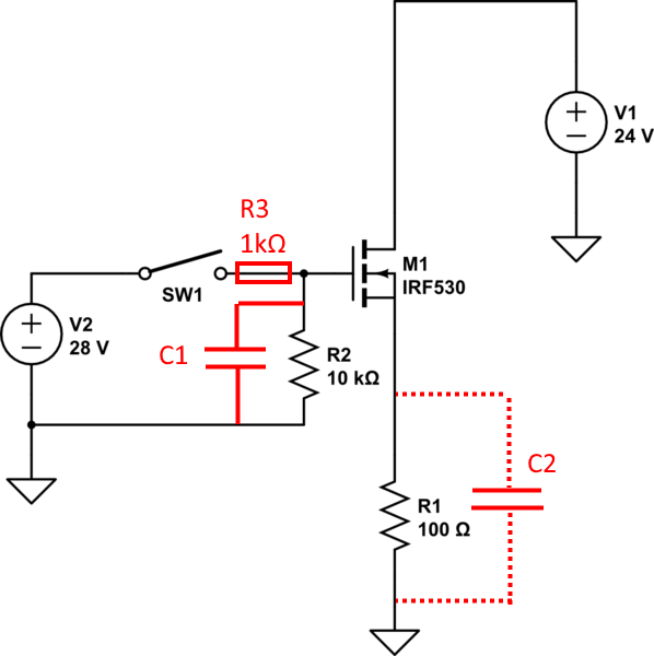
Driving the gate of a high-side N-channel MOSFET is not a new problem, and there exist many solutions. A couple of simple changes to your proposed circuit could be workable, refer to the red mark-ups in the image below:
enter image description here

What we need to do is prevent the gate voltage going high faster than the source voltage. A simple RC delay circuit may be sufficient for this, I have added R3 and C1 to your original circuit. The trick here is to make the time-constant at the gate drive to be much longer (slower) than any time-constant on the load side of the MOSFET. The time-constant of the load side is formed by the load device, and any parasitic capacitance it may have (as indicated by the dashed lines to C2), including the parasitic capacitances of the MOSFET.

Putting some typical values in: Let's say that C2 = 1nF.
The time-constant on output is R1.C2 = 100Ω x 1nF = 100ns.
Let's make the time-constant at the gate to be 10 times this, ie: 1us.
At turn-on, the time-constant is R3.C1, so C1 = 1us / R3 = 1us / 1kΩ = 1nF.
At turn-off, the time-constant ie R2.C1 = 10kΩ x 1nF = 10us.

Conclusion:
For both turn-in and turn-off, the time-constant of the gate-source drive is much longer (slower) than that at the MOSFET output terminals, (Source, and Drain), so we have achieved our goal. This means the gate-source voltage will not exceed the maximum rating at any time.

But there is a problem: R3 and R2 form a voltage divider, so the highest voltage that the gate can reach will be: 28V x (10kΩ / 11kΩ) = 25.45V, which is only 1.45V above the drain voltage of 24.0V.

Now, this may or may not be OK - it depends on what you're trying to do. If you want to switch much faster than this, then this is not the solution you need.

To explore other solutions, these links may be a good starting point:

Driving a P-channel MOSFET with high voltage input

https://electronics.stackexchange.com/a/710378/341959
\$\endgroup\$
0
\$\begingroup\$

There is no problem if the load is a resistor as shown in the example. But if there is some capacitance in the load it may keep the voltage high for some time after the gate is switched to zero and then you exceed the max Vgs.

It would be better then to protect the MOS with (for instance) 2 back-to-back Zener diodes between source and gate, and a series resistor between the gate and V2 to protect those Zener diodes if the driving source (V2 in the example) is not internally limiting the drive current enough already (in the example that is not shown).

\$\endgroup\$
1
  • \$\begingroup\$ Good point! (I meant back-to-back Zeners, not anti-parallel of course...) \$\endgroup\$ Commented May 24 at 21:55

Your Answer

By clicking “Post Your Answer”, you agree to our terms of service and acknowledge you have read our privacy policy.

Not the answer you're looking for? Browse other questions tagged or ask your own question.