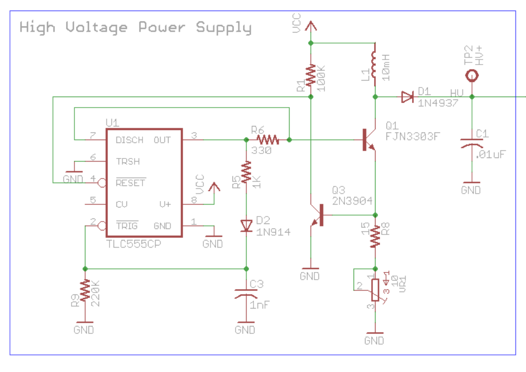
I know a bit about boost converter design, so Q1 switching on and off from the output of the 555 timer makes sense to me. What doesn't make sense is how the 555 timer is working in astable mode. C3 is not getting charged through two resistors like is commonly seen in 555 timer datasheets. Is it operating differently than I think or am I possibly just missing something?
-
1\$\begingroup\$ I mean, whether you use a resistor or the collector-base junction of Q1 to pull up OUT, does it make a difference? What surprises me is that Jeff Keyzer used a 555 for this, which makes it quite an atypical circuit for the purpose, and unnecessarily component-rich (read: hard to assemble). An equally ancient and cheap and available 34063 (originally probably MC34063, but there's clones from very many companies, AZ34063, KA34063, SP34063…) would have actually solved the feedback problem and could also have been used with an external switching transistor. \$\endgroup\$– Marcus MüllerCommented Jul 28 at 10:00
-
1\$\begingroup\$ (and of course, if he was in the business of building supplies for manufacturing, he might have chosen a modern step-up converter IC, but seeing he builds kits for hand-assembly, sticking with DIP ICs is probably the way to go, so MC34063 would be a reasonable choice) \$\endgroup\$– Marcus MüllerCommented Jul 28 at 10:08
3 Answers
I think that pin 3 must be HI when \$Q_1\$ is active. This happens right away because \$C_3\$ is initially discharged and therefore the internal RS FF is actively being SET. The base of \$Q_1\$ can't be more than two diode drops above ground. So the remaining voltage sits across \$R_6\$ to produce about \$5\:\text{mA}\$ of base current into \$Q_1\$.
That will pinch \$Q_1\$ such that about \$1.6^+\:\text{V}\$ is across \$L_1\$, yielding about \$160\:\frac{\text{A}}{\text{s}}\$. Ignoring the potentiometer for now, when the current in \$R_8\$ reaches about \$40\:\text{mA}\$ (the current in \$L_1\$ being about \$35\:\text{mA}\$ then, for \$\beta=7\$), \$Q_3\$ goes active and actively clears the RS FF to RESET and so pin 3 goes LO (as does the now-active pin 7 discharge, too), shutting off \$Q_1\$. All that should happen in about \$220\:\mu\text{s}\$, or less, and \$L_1\$ now discharges via \$D_1\$ into \$C_1\$.
While pin 3 was HI it rapidly charges \$C_3\$ via \$R_5\$ and therefore removes any active reset going to the RS FF, which holds its current state. (Pin 6 is grounded, so it cannot affect the RS FF.) This takes only a microsecond, or so. But provides managed protection to prevent noise or disturbances from changing pin 3's HI state, for a short time.
When pin 3 goes LO, \$C_3\$ discharges out through \$R_9\$ with a \$220\:\mu\text{s}\$ time-constant. \$D_2\$ had ensured that it didn't charge to higher than about \$2.4\:\text{V}\$ to start. That's convenient because it means it will take about one time constant to reach about 63% less, which is about where the trigger goes active, again. Probably about \$200\:\mu\text{s}\$? That causes the RS FF to be actively SET.
So this part of the cycle gives about \$200\:\mu\text{s}\$ time for \$L_1\$ to fully discharge. That handles the worst case, which will be the first few cycles that \$L_1\$ experiences. It won't be long, though, before the voltage across \$L_1\$ during its discharge into \$C_1\$ will be very, very short as the voltage across \$C_1\$ increases. And so, less time will be required soon. But that rest-time will be imposed, regardless, as there's nothing to detect when \$L_1\$ is discharged and to feed that back to shorten pin 3's OFF period.
The timing are all ball-park. But it's on the order of a few hundred microseconds per half-cycle.
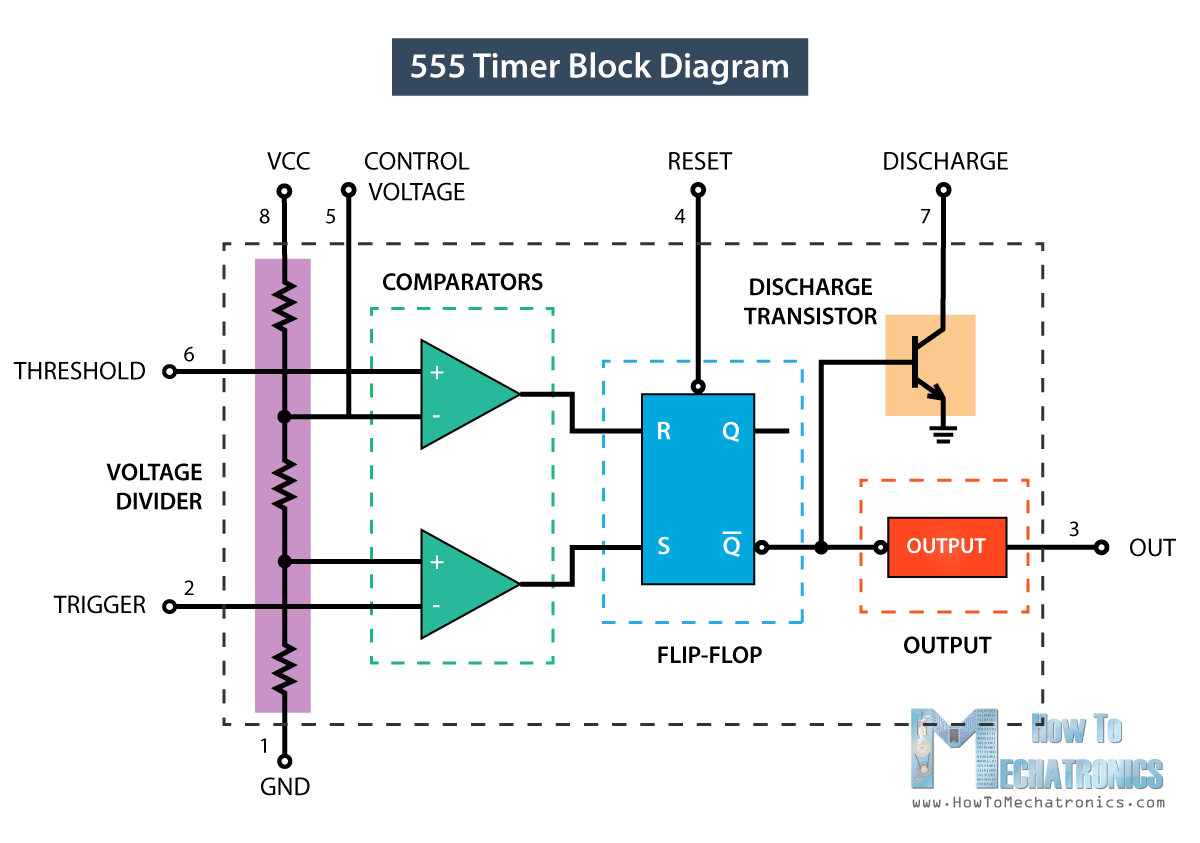
The internal diagram of a 555 can help:
Img nicked from here
There are two comparators, top and bottom as you can see, which have their reference voltages taken from the divider i.e. 2/3 and 1/3 Vcc, respectively.
The outputs of these comparators (R and S) go to an asynchronous RS flip-flop (RSFF). The truth table of the RSFF is:
| R | S | \Q (Q-bar = inverse of Q) | OUT (inverse of Q-bar = Q) |
|---|---|---|---|
| 0 | 0 | Hold (No Change) | Hold (No Change) |
| 0 | 1 | 0 | 1 |
| 1 | 0 | 1 | 0 |
| 1 | 1 | Invalid | Invalid |
Because the THRESHOLD pin (pin-6) is at 0V, the top comparator will always output 0, therefore, R will always be 0. So the top two rows above are of interest.
When the power is first applied, the capacitor is empty and the non-inverting input of the bottom comparator is at 1/3 Vcc, so the bottom comparator will output high so S = 1. So the OUT will be 1 and the transistor Q1 will be on.
When the OUT is on, the capacitor C3 will charge through R5 (R9 has almost no effect on charging here). Once the voltage across C3 hits 1/3 Vcc or goes slightly beyond it the bottom comparator will output low so the S input will be 0. This makes R = S = 0 so the OUTPUT will stay on (Hold state).
Whilst the transistor Q1 is on (because OUT is high) the current through L1 will ramp up and develop a voltage across R8 and VR1. Once the voltage here hits 0.6 ~ 0.7V (takes 80 ~ 130 μs for VCC = 3V, depending on the VR1 position) the transistor Q3 will turn on and reset the RSFF. This makes the \Q high (because Q will be 0) so the DISCHARGE transistor quickly turns off the transistor Q1.
Once the Q1 transistor turns off, due to the flyback action of L1 there's going to be a voltage across the TP2 and it'll be higher than the input, VCC. RESET pin becomes high again (through R1 pullup) and enables the RSFF, and C3 starts to discharge through R9. Note that the voltage across C3 should have reached VCC already because the transistor Q1 is kept high for a long enough time compared to the time constant τ = R5 x C3. Once the voltage here reaches 1/3 Vcc or drops slightly below it (takes ~200 μs for VCC = 3V input) the bottom comparator outputs high and this makes S = 1 and therefore turns on the transistor Q1. And the cycle starts afresh.
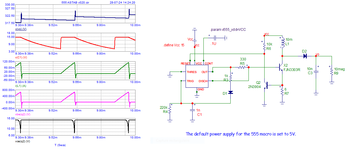
Made with microcap v12
The circuit "can't" work if the supply voltage is too low ( < ~12 V).
With 15 V, it works with R8 and UR1 (my R7) varying current into the self and fixing output voltage.
It takes some time for a "stabilized" output.
-
1
-
1\$\begingroup\$ I don't know. Result of simulations, 555 model perhaps faulty. Under 12 V, the simulation show a modified behavior. I have not deepened. \$\endgroup\$ Commented Jul 28 at 19:27
-
1\$\begingroup\$ is it possible a bipolar 555 model? this is a CMOS 555… \$\endgroup\$ Commented Jul 28 at 19:28
-
1\$\begingroup\$ My 555 is a "macro" circuit idealized. tried also with a TLC555 CMOS. Same behavior. \$\endgroup\$ Commented Jul 28 at 19:39


