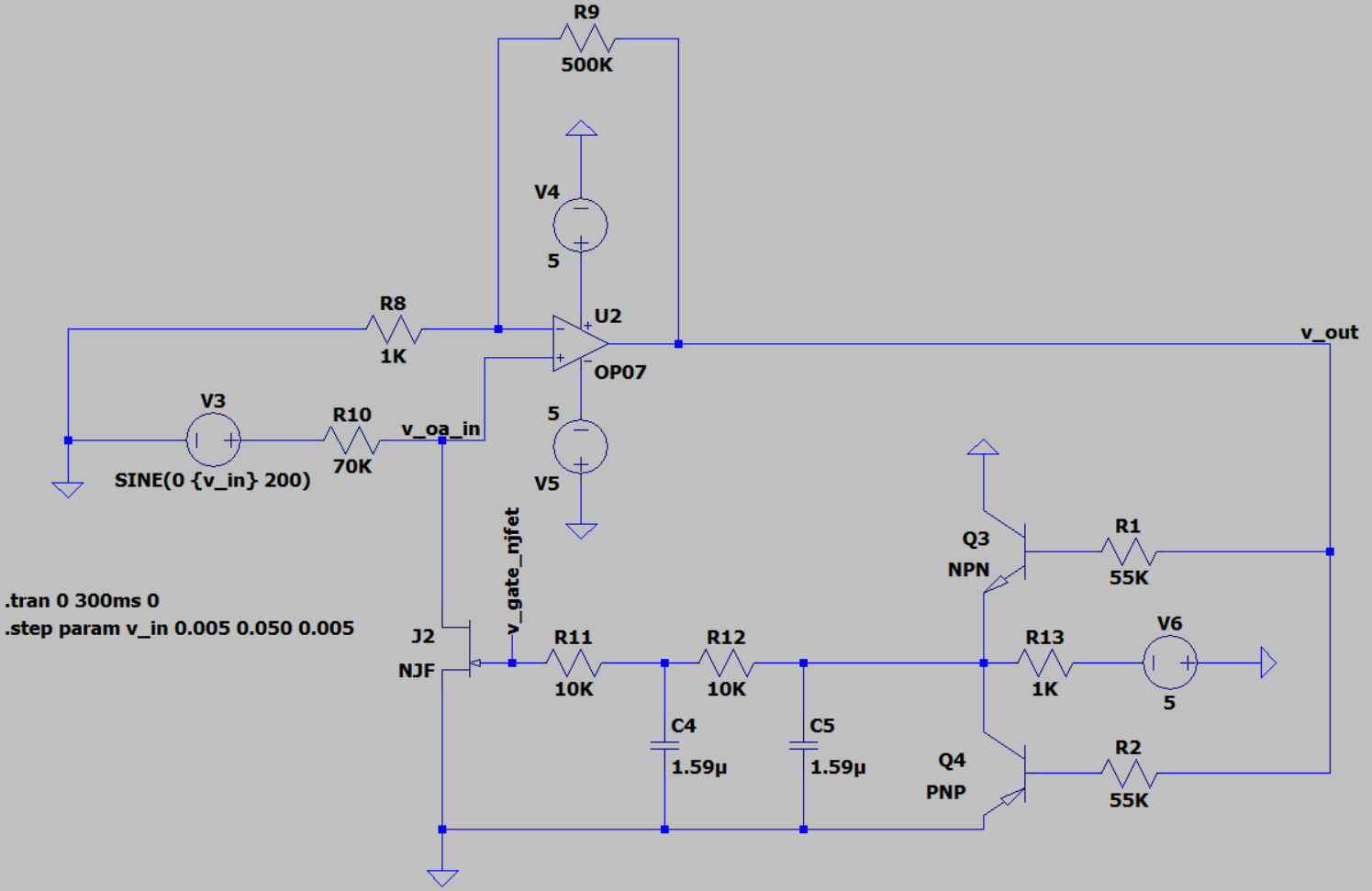
I am working on the schematic below. My goal is to create an automatic gain control circuit which can handle inputs from around 5mV to 50mV and amplify them to be in the neighborhood of 2-3V.
The theory of operation for this AGC is that NJF and R10 create a resistive divider at the non-inverting input of OP07 which has a constant voltage gain of 500 (54ish dB). Depending on the output of OP07 a variable DC voltage will be present at the input of NJF's gate. This variable voltage changes the resistance of the gate. negative voltages lead to very high impedances so that v_in is approximately equal to v_oa_in. As the gate voltage approaches 0v the resistance decreases and a larger voltage drop occurs across R10
This project is mostly for experimentation so a lot of my goals are arbitrary. One of my arbitrary goals was to try to get 20 dB of variable attenuation on the input signal. I did this in two ways...
First I can always increase R10. The detriment of this is that I essentially increase my minimum attenuation, but I also increase the dynamic range of my variable attenuator.
Ex. Lets say the NJFETs resistance varies from 50K to 5K.
If R10 = 10K min_atten = 50K/(10K+50K) = 5/6 = 0.833 = -1.58dB max_atten = 5k/(10K+5K) = 1/3 = 0.333 = -9.54 dB
Dynamic Range is approximately 8 dB
If R10 = 50K min_atten = 50K/(50K+50K) = 1/2 = -3dB max_atten = 5K/(50K+5K) = -20.82 dB
Dynamic Range is approximately 17 dB
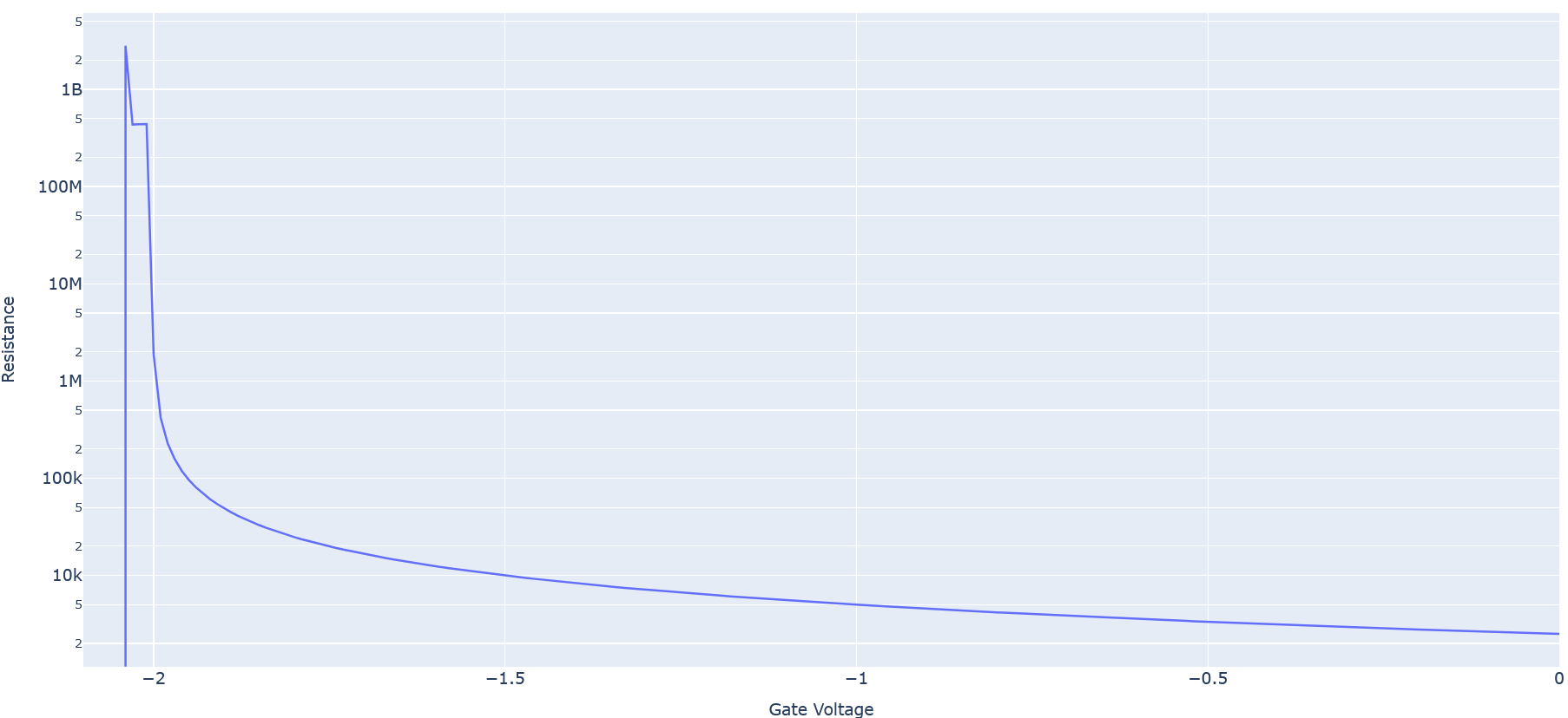
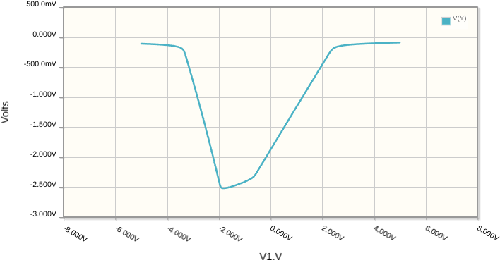
Second, I can increase dynamic range by adjusting R1 and R2 which limit the current through drain Q3 and Q4. Limiting Q3/Q4s collect/emitter current leads to less voltage drop across R13 which leads to a more negative voltage at v_gate_njfet. Per the sweep of gate voltage vs resistance below, if I can get v_gate at my minimum input signal to be near -2V I should have much more dynamic range for my variable resistance. It turned out that for my input voltage ranges R1,R2 = 55K pretty much did exactly that.
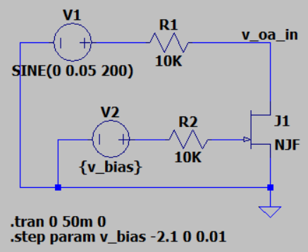
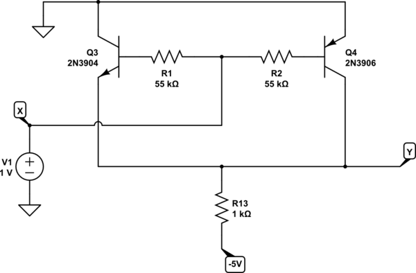
Note the figure above was generated using the circuit below. Where I defined the resistance as R = V(v_oa_in)/I(R1)
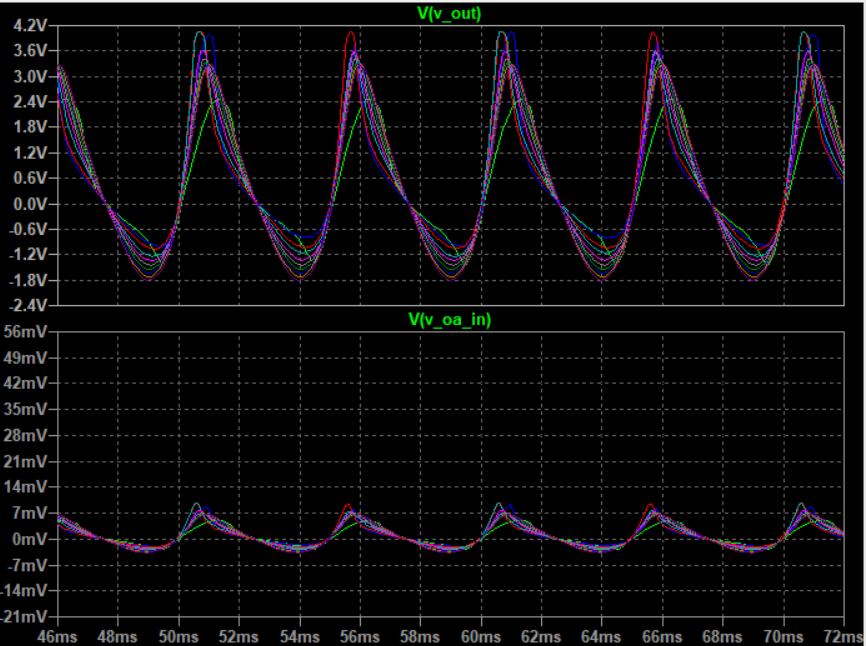
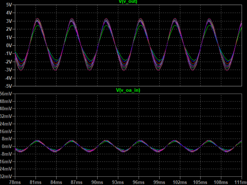
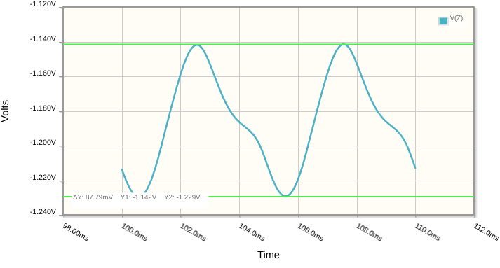
So at this point I was at a dynamic range of about -17.5 dB with a minimum attenuation of almost 0 dB. I am pretty happy with this but wanted to see if I could adjust R10 further to get a better dynamic range so I adjust from R10=70K to R10 = 100K then 500K. At 500K I notice that my output signal looks terribly distorted see the image below.
My question is what is causing this distortion? I know that non-ideal op-amps will draw some amount of current at their inputs in order for the amplifier to work correctly. I wonder if my input resistance is too high and prevents the op-amp getting the bias current it needs?
For reference with R10 = 70K the signal is below. Still some distortion but not nearly as bad. (I really need to take an FFT to check how bad the distortion is but I haven't done that yet)
Although not the purpose of the question I am open to hearing feedback on my design, I know there are other approaches to AGC which use a variable gain amplifier rather than a variable attenuator followed by a constant gain amplifier.
Thank You
EDIT_1
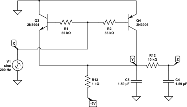
There appears to be some confusion in what transistors Q3 and Q4 are doing so I am including some additional information here. I'll preface this by saying this is my first time designing something like this so if there are any obvious pitfalls/incorrect statements in the following explanation please correct me.
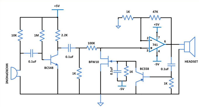
My AGC circuit design started out in this article. In this design the author uses a BC558 PNP transistor to essentially pull the node left of R13 up towards 0V when the signal v_out is at its gate. Essentially it acts like a half-wave rectifier allowing current to flow when the base of the PNP is -0.7V relative the emitter. What I tried to do was create a full wave rectifier using a PNP and an NPN. The goal being that the NPN would conduct on the positive portion of the sinusoid while the PNP would conduct on the negative portion of the wave. In hindsight I could probably go back to only the PNP transistor but when I initially made the change I was using the circuit in the image below and was having trouble getting the 0.1uF capacitor to stay charged for the entire period of the wave without large swings. I was hoping that by rectifying both positive and negative portions of the wave I could solve that issue.
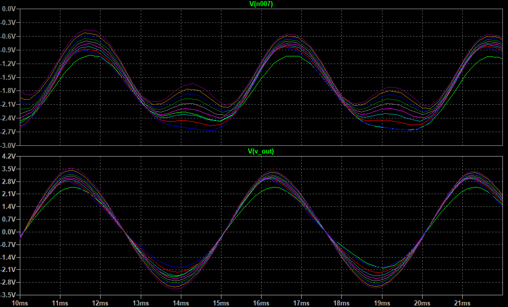
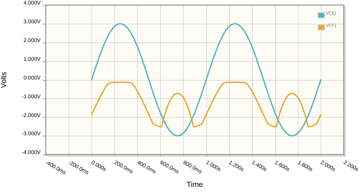
Since I changed my circuit from the above though I could probably use only one of the PNP/NPN transistors. Per the image below my "full-wave" solution doesn't really create a "full wave" it is skewed more which suggests the PNP transistor conducts more then the NPN. V(n007) is the node to the left of R13

