7
\$\begingroup\$

I'm reimplementing an 80's-era controller board for which I have schematics but no gerber files; the original board has damaged traces so I'm trying to stick mostly to the original design, with modern upgrades in only a select few places.

One series of driver circuits I'm not fully understanding is this Darlington-PNP arrangement (https://arcarc.xmission.com/Pinball/PDF%20Pinball%20Misc/Williams%20System%2011b%20Schematics.pdf) existing design
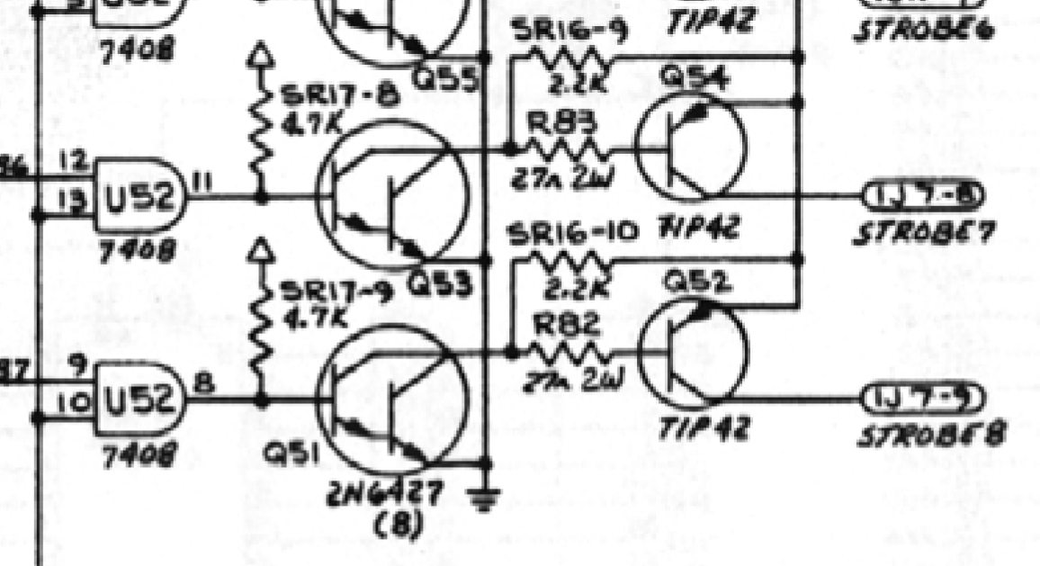
The high side of the PNPs here is driven by 18VDC. I would like to eliminate the 2W resistors here because they were a source of thermal stress on the original board, so ideally I would be replacing the entire chain after the logic gate with a single MOSFET. Other driver circuits (controlling solenoids) I've replaced with N-Channel MOSFETs with success, but I'm not sure if they're trying to accomplish some unseen voodoo here with the PNP drives - are they current-limiting the output? Are the PNPs operating in the saturated region here? These are driving incandescent lamps, so nothing fancy on the outputs (unless they're over-driving the lamps with 18V but current-limiting them?). The lamps are being used as "flashers", so are only on for ~100ms at a time.

Thanks

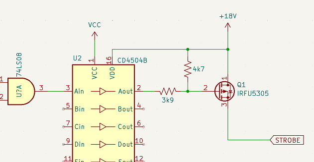
EDIT 1: Ok, so what about this? Again, trying to stay as true as possible to the original as far as output behavior (would like to have 18V instead of 12). A 4504 would safely translate my logic levels into the 18V range, so I can drive the FET directly, no? Or, perhaps I could change over to AND gates with open-collector outputs?

Alternate solution?

EDIT 2: Erk...I was mis-reading the schematic and thought the divider was on the source and not the gate. Now I follow. Thanks again.

\$\endgroup\$
4
  • 1
    \$\begingroup\$ The company is defunct via a series of acquisitions, but the schematics were published in the documentation that was included with every unit sold. This was back when service techs were actually encouraged to debug and resolve component-level issues with the CPU boards. \$\endgroup\$
    – ereisch
    Commented Nov 24 at 6:19
  • 1
    \$\begingroup\$ Are the PNP transistors on a heatsink? If they're current limiting, they should dissipate a lot more than if they're saturated. \$\endgroup\$
    – bobflux
    Commented Nov 24 at 8:11
  • \$\begingroup\$ No, they aren't. The ceramic power resistors are what's generating all the heat. \$\endgroup\$
    – ereisch
    Commented Nov 24 at 15:15
  • \$\begingroup\$ Then most likely no current limiting and no risk to use Simon's solution. You could also replace the incandescents with LEDs. \$\endgroup\$
    – bobflux
    Commented Nov 24 at 16:11

2 Answers 2

7
\$\begingroup\$

It doesn't seem like there are any current-limiting measures going on there. I suspect that the 100ms on-time for the lamps is too short for a 12V lamp to light quickly enough. Perhaps they require closer to 18V to get it to illuminate more quickly, but because illumination time is so short, average lamp power is acceptably low.

I think there's something similar going on with the 2W resistors, which seem to be 27Ω. With their corresponding lamps lit, they will have close to 17V across them, for a power dissipation of \$\frac{(17V)^2}{27\Omega}=11W\$. If that lasted much longer than a few hundred milliseconds, they would be toast in short order. The designers seem to be relying on average power to be under 2W, and are not so concerned with peak power.

You won't be able to replace the darlington pair and the PNP with a single P-channel MOSFET, because that MOSFET will require +18V at its gate to switch off. The 7408 simply can't do that, and you will still require level translation from TTL to 0V/+18V.

I also wouldn't be comfortable having a fast 18V transition at the MOSFET drain coupling via gate capacitance directly to the 7408's output.

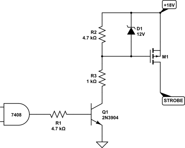
For those two reasons, I think you should still have an intermediate NPN transistor between AND gate and MOSFET:

schematic

simulate this circuit – Schematic created using CircuitLab

18V is close to (or beyond) the maximum \$V_{GS}\$ for many MOSFETs, so I've used R2 and R3 to cut \$V_{GS}\$ to 14V or so. D1 may not be necessary if the loads (at STROBE) are gentle, and the power supply is stable, but it will add another layer of protection for the MOSFET.

I use a BJT (Q1) because the 7408 will almost certainly never output +5V. Its high output could be as low as +2.4V. That's a little low for switching a typical N-channel MOSFET gate, the BJT is a better fit, and arguably better protection for the AND gate from the load.

I haven't considered switching speed at all. This is likely to be marginally slower compared to the original BJT implementation. Nothing here dissipates more than 50mW, except M1, which you choose to have an appropriately low \$R_{DS(ON)}\$ when \$V_{GS}=-12V\$, for acceptable power dissipation while passing whatever load current is expected.

\$\endgroup\$
2
\$\begingroup\$

Tod need a couple of MOSFETs to replace this configuration, a small signal n-channel in place of the Darlington and a p-channel to replace the PNP. You’d replace the 27R with something rather larger and add a pull-up to allow the p-channel FET to switch off. Whether the resistor is current-limiting depends on the current gain of the PNP. 27R across 18V indicates a base current of more than 0.5A so unless the output current is very high I’d think that the PNP would saturate, although it may provide transient current limiting for a cold filament. You could achieve something similar with an RC to slow the switch-on time.

\$\endgroup\$

Your Answer

By clicking “Post Your Answer”, you agree to our terms of service and acknowledge you have read our privacy policy.

Not the answer you're looking for? Browse other questions tagged or ask your own question.