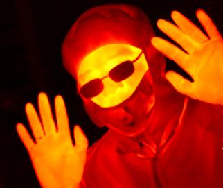
We're finally starting to see practical thermal imaging sensors (microbolometers) entering the consumer market. However, they are still vastly more expensive than comparable visible imaging sensors. The most basic 384x288 17µm pixel (i.e., 32mm2) thermal imagers run about $500, whereas $500 will get a 6000x4000 2µm pixel (i.e., 96mm2) CMOS sensor ... plus 5-axis sensor stabilization and more.
My question: Assuming the same economies of scale were applied as are already used for conventional CMOS sensors, is the manufacturing process for silicon microbolometers inherently more expensive? Or in the limit is it still just some (similar) number of photolithographic steps?
To elaborate: Thermal cameras look for radiation with wavelengths between 7-14µm, whereas visible light is in the range 0.4-0.7µm. Based on the physics alone, at the diffraction limit microbolometer pixels will have an order of magnitude greater surface area. Apparently commercial sensors are at the diffraction limit for both visible light (at 1 micron pixels) and thermal light (at 17 micron pixels). So, to make it fair, we might compare a 1" 24Mpx visible sensor with a 1" 300kpx thermal sensor.
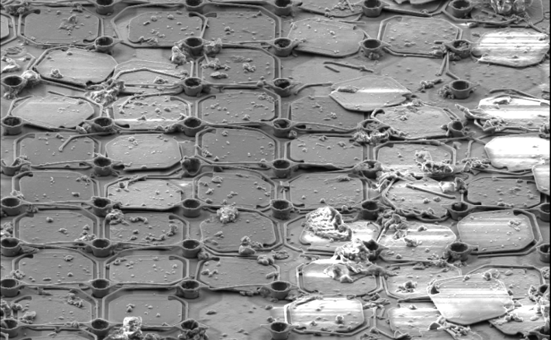
Both sensors can be made from silicon using a CMOS process. The structure of microbolometers looks a little trickier than state-of-the-art visible spectrum CMOS sensors, requiring a thermal bridge for each pixel as well as vacuum encapsulation of the sensor. But I know little of large-scale manufacturing processes, so are these variables significant in the limit on a per-unit basis?


