0
\$\begingroup\$

I have been reading about switched-mode DC-DC converters and I'm having some trouble fully understanding the behaviour.

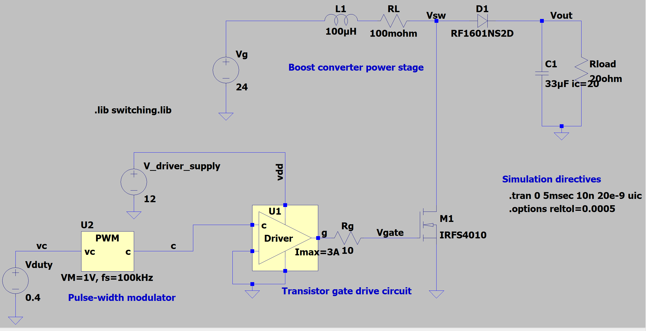
Take the following circuit for example (no feedback loop):

enter image description here

enter image description here

I understand there are a few things happening here:

  1. The switching frequency of the converter should be much higher than the cut-off frequency of the LC low-pass filter. This is to ensure that we (ideally) do not see the switching frequency or harmonics of the switching frequency at the output. Of course, there will be some attenuated output voltage ripple that does make it through. This is what allows us to use the small-signal approximation.
  2. The LC filter has a 2nd order time domain response which should be a decaying sinusoid, is that what we see in the initial transient of the simulation?

Why do we not see this decaying sinusoid every time the switch switches - that should be like applying a step input to the filter each time, correct? Can someone explain to me where the initial transient response is coming from and when do we consider the time-domain response of the LC filter?

\$\endgroup\$
9
  • 1
    \$\begingroup\$ A DC-DC converter is a control system with feedback. The feedback frequency response is designed in such a way that it damps out the natural response of the LC filter. Normally the period of the LC response is much longer than the switching period, so the loop has plenty of time to negate the natural response. This is part of stabilizing the DC-DC converter. If you use a fixed duty cycle DC-DC converter (with no feedback), you will see that the natural response is present and UN-damped under no-load conditions. If there is a load, the load damps out the LC response. \$\endgroup\$
    – user57037
    Commented Dec 27, 2020 at 23:51
  • 1
    \$\begingroup\$ Yes. Applying 9.6V step, or applying 24V at 0.4 duty cycle will give you almost the exact same response (other than the slight remnant of the switching frequency). Take a look at my answer to this question: electronics.stackexchange.com/questions/532430/… \$\endgroup\$
    – user57037
    Commented Dec 28, 2020 at 1:06
  • 1
    \$\begingroup\$ Ah!! So essentially, the switching frequency is so much larger than the natural frequency of the LC circuit that the LC circuit only sees a 24V at 0.4 duty cycle or a 9.6V STEP! and hence the response is that of a 9.6V step! The LC simply does not care about the rapidly switching 0V - 24V - 0V since the frequency is too high and is filtered out. \$\endgroup\$ Commented Dec 28, 2020 at 1:16
  • 1
    \$\begingroup\$ Exactly. You can generally pretend that the Voltage at the filter (the switching node) is Vin * D (where Vin is the input to the regulator). NOTE: this is only strictly true during synchronous switching or continuous current mode. If you have a diode as a low-side switch, and the duty cycle is low, then the analysis may be a bit different. \$\endgroup\$
    – user57037
    Commented Dec 28, 2020 at 1:26
  • 1
    \$\begingroup\$ Sorry, small-signal approximation is the term they used in the book to say that we can assume the Vout of the converter is = to the DC D*Vin and we can ignore the effect of the switching harmonics going through the LC filter and causing a small-signal ripple on the output of the converter. \$\endgroup\$ Commented Dec 28, 2020 at 2:10

3 Answers 3

2
\$\begingroup\$

Why do we not see this decaying sinusoid every time the switch switches - that should be like applying a step input to the filter each time, correct?

While it is a step-like action, the time constants differ by a very large amount. The step response of the (R)LC filter is dictated by its natural frequency, which is much lower than the switching frequency. Simply put, you're looking there at ms worth of time, while the pulse width is less than 10 µs. Plus there are other factors at play.

Can someone explain to me where the initial transient response is coming from

First, you chose an interesting combination of values. If you look at the trace for the inductor current, you'll see that it starts in CCM, but then it goes into DCM immediately after the first peak, only to continue in CCM afterwards. This complicates things a bit.

As it is, the whole power stage can be simplified to be an RLC filter, with modified values according to the duty cycle. The ideal CCM transfer function for the boost converter is \$M=\dfrac{1}{1-\alpha}\$ which, for your value of 0.4, it means 1.67 times the input voltage. The inductor will charge with energy during the ON time, and release it during the OFF time (as opposed to all the time, like a mains transformer). The capacitor, too, while the load will be proportional to M. In addition, modelling the input source to be a step source of 24 V times M, will result in the following equivalent circuit:
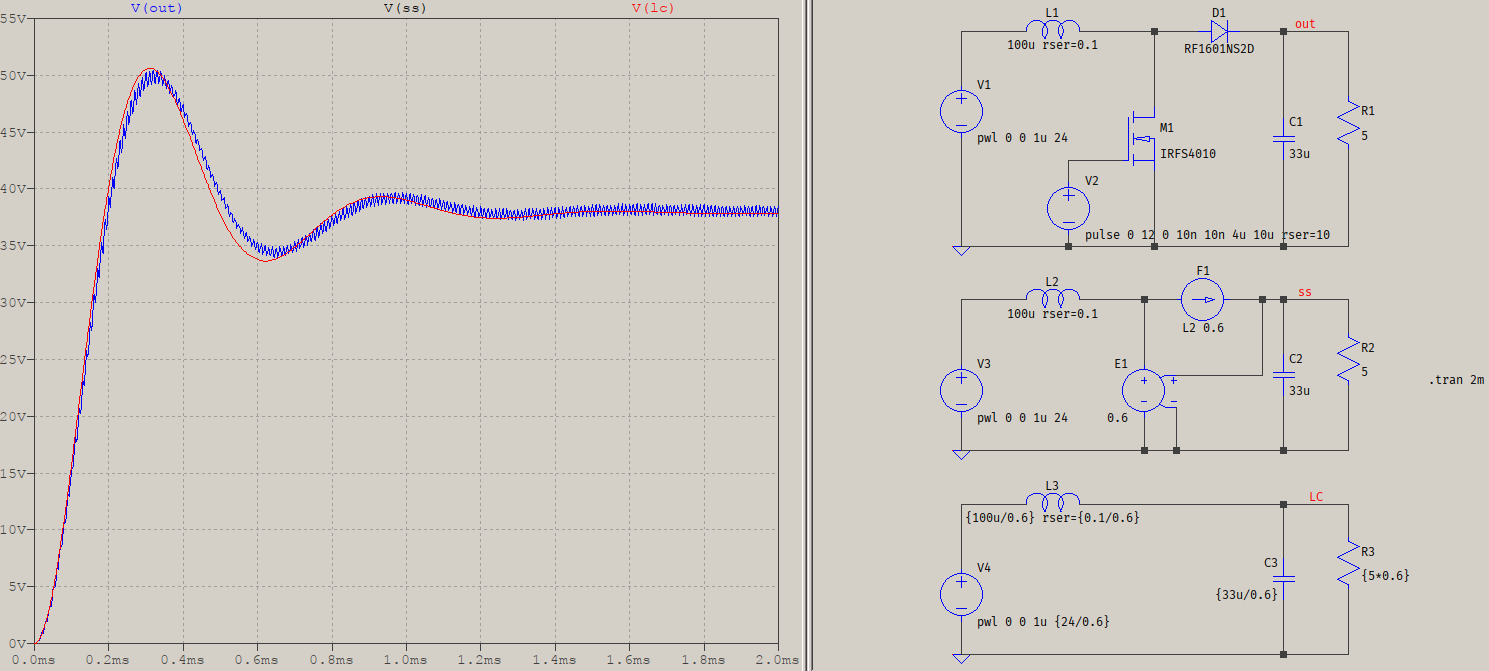
test

The upper one is your circuit (V(out), blue), the middle one is a small-signal model (V(ss), black), and the bottom one is the RLC equivalent (V(LC), red). If you can't see the black trace it's because it overlaps with the red trace. There are small differences between the switched waveform and the rest due to the MOSFET's and diode's ON/OFF resistances & co.

Now, because of the mix of modes that your initial values presented, I had to choose a different value for the load (5 Ω), to ensure CCM everywhere. Otherwise it would have looked like this:
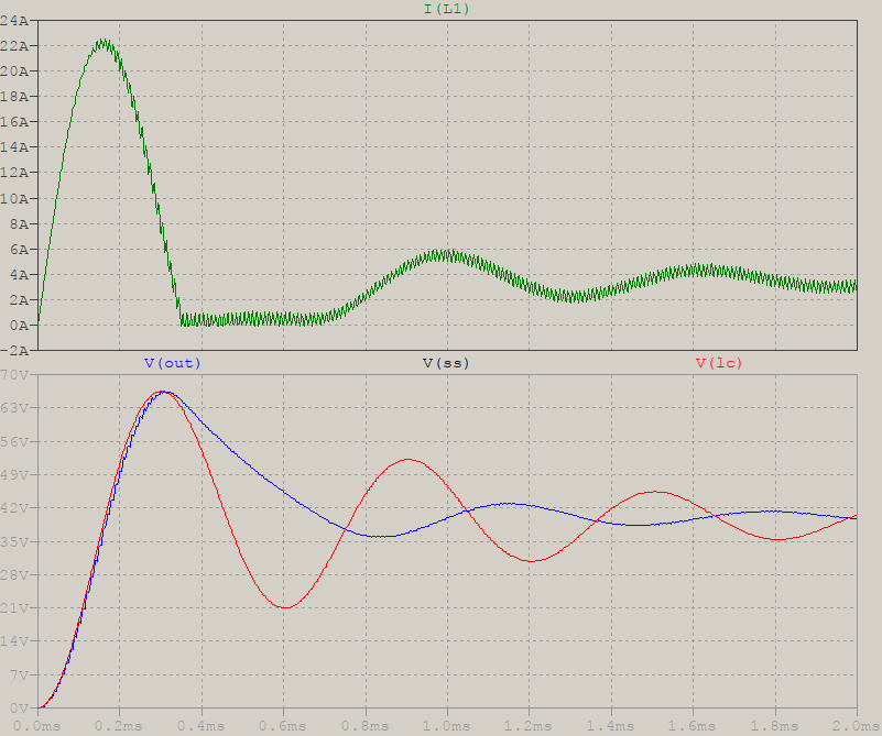
mix

As you can see, the waveforms (almost) coincide until the DCM part; then, all bets are off. The small-signal model can be adapted to the situation, which would require some conditionals, but the RLC circuit is linear.

when do we consider the time-domain response of the LC filter?

This question is very vague, and impossible to answer. You'll have to decide what you really want to know.


I've modified the small signal model to include DCM operation, so now it is apparent that the DCM operation is nonlinear and, thus, the simple RLC approach is unsuited:
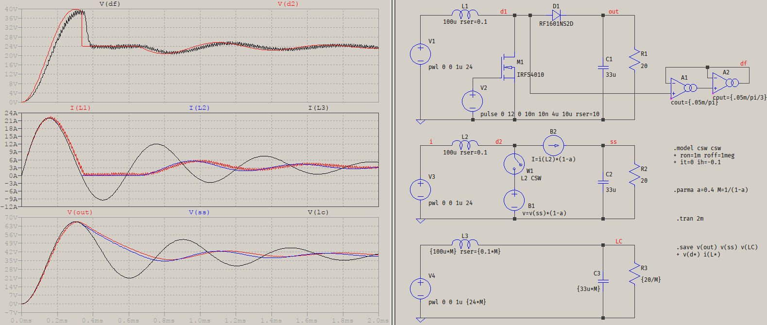
DCM-ss

W1 disconnects B1 when the current through L2 drops below zero, so it appears that the equivalent drain voltage is open. A1 and A2 form a Bessel lowpass to filter out the switched drain voltage of M1, showing in the upper plot pane the comparison of the average of V(d1) (with a slight delay due to the filter) with V(d2), which is the small-signal equivalent. Since a time-varying resistor is involved, there cannot be a linear equivalent of the circuit with an RLC only.

The conclusions remain (as mentioned in the comment below):

  • the undamped response is because the overall transfer function of the converter (without feedback) is largely dominated by the output LC filter and the equivalent resistance/impedance as the load, thus the switched mode step response can be replicated by an equivalent linear RLC circuit, as long as there is no DCM involved.
  • the switching, itself, is just like applying a step, each time, but the duration of that step is very small compared to the period of the natural frequency of the filter.
\$\endgroup\$
4
  • \$\begingroup\$ "While it is a step-like action, the time constants differ by a very large amount. The step response of the (R)LC filter is dictated by its natural frequency, which is much lower than the switching frequency." - But, how come it happens in the first place then? The switching frequency is what is connecting the 24V to the LC filter from the start. Is it because of the extremely high di/dt at the start since there is no current in the inductor? \$\endgroup\$ Commented Dec 28, 2020 at 0:47
  • \$\begingroup\$ It's possible that my English is not that clear, but the whole response is about comparing the "raw" RLC with the boost power stage: for a non-feedback CCM, the responses are the same (provided you make the equivalent RLC values), while for DCM it's not possible due to the inherent linearity of the RLC (DCM, being discontinuous, is nonlinear). Feedback linearizes the transfer function, which means damping; without it, the system's transfer function is, largely, dominated by the RLC transfer function. Even with it, but the loop changes the behaviour. \$\endgroup\$ Commented Dec 28, 2020 at 8:20
  • \$\begingroup\$ I've updated my answer, maybe it's clearer now. \$\endgroup\$ Commented Dec 28, 2020 at 10:46
  • \$\begingroup\$ Re-reading now I see I should have added that what I present as a DCM averaged model is, in fact, an approximation: it won't let the current go below zero, but it does drop to zero, which doesn't happen in DCM. \$\endgroup\$ Commented Feb 5, 2021 at 16:56
0
\$\begingroup\$

The waveform shows current leading voltage thus inductive current

  • L=100uH , dI = 13 A , dt = ~ 0.1 ms to 1st current peak when V~38V

  • V=LdI/dt = 100e-6 * 13A / 0.1ms = 13V which is the difference between 24Vdc in and 38Vdc approx.

This accounts for the rise time approx. to the step input Voltage, but not the pulse PWM which is a shorter cycle.

more clarification.

  • The initial Step on for 24V has a series RLC response with high Q since ESR is near 0 (DCR (L)=0.1, Rs(D1)<=0.1 Ohm

  • The resonant frequency is near 2kHz where L=100uH has an impedance < 1 Ohm thus giving a Q of ~ 5. This is appropriate for the observed resonant decay time.

  • The high surge current thus promotes the desire for a soft start circuit with slightly more turn-on time. This would be implemented with an additional series PWM controlled switch which becomes the classic Buck/Boost circuit.

  • However the Switcher at 100kHz makes the ZL(100uH)=50 Ohms in series with the 20 Ohm load shunted by 39uF which Zc < 0.1 Ohm (33uF @ 100kHz). Thus the impedance ratio would appear to be well damped.

\$\endgroup\$
4
  • \$\begingroup\$ I understand. But, why does this happen only in the beginning? The switch causing the inductor voltage to switch between the Vg source and 0V very fast from the beginning. So shouldn't we see the ripple at each switching event? Or the ripple should not happen at the start either. \$\endgroup\$ Commented Dec 27, 2020 at 22:56
  • \$\begingroup\$ This is a one time 24V Step response. The switch draws current for a short duration dt thus has a smaller dV and dI \$\endgroup\$
    – D.A.S.
    Commented Dec 27, 2020 at 23:25
  • \$\begingroup\$ What I mean is that that 24 Vg source is appearing at the input of the LC filter through the switch. So why do we not see the 24V step response ripple every time the switch is on. Why is it only at the start if the switch is always switching from the start. \$\endgroup\$ Commented Dec 27, 2020 at 23:34
  • \$\begingroup\$ i presume you understand reactance/R ratio as Q and it meaning \$\endgroup\$
    – D.A.S.
    Commented Dec 28, 2020 at 0:57
0
\$\begingroup\$

Someone has set 20V intitial voltage to C1 but L1 has initial current =zero. That's obscure combination, but it's there, so it is the starting point. I would assume the initial voltage to be either zero or 24V minus voltage drop in coil and diode.The latter version would need about 1200mA initial current for L1.

The current is built to L1 gradually because M1 connects it regularly to 24VDC and as long as the output voltage is less than 24V nothing decreases L1 current. After Uout is over 24V the current of L1 starts to drop, but the output voltage still grows. Uout starts to drop when L1 current has dropped to zero. The voltage drops due the load current.

One switching cycle has not enough time to build very large current change. It takes some time until the switching builds enough new L1 current to charge again C1 so much that there's visible voltage rise.

Finally the oscillation of the LC circuit settles. Due the high switching frequency L1 current danses around the output current when the initial transient is died.

I have 3 suggestions:

  1. Learn in details how inductor current grows or decays if there's voltage between its terminals. Know that inductor itself generates as much voltage as needed to allow the current to change gradually. This is how boost regulator makes the voltage higher. Inductor current change rate A amperes per second needs voltage A*inductance in henries.

Learn also the dual version of that phenomen: The voltage of a capacitor never grows nor drops stepwise, voltage change rate A volts per second needs current A*capacitance in farads.

  1. Learn what happens if M1 stays non-conductive but you start from zero Uout and zero L1 current. You see LC transient but it's somehow faster because you do not disturb it by switching L1 repeatedly to 24V from charging C1.

  2. Get an elementary text of sw.mode power supply principles. You will soon learn that L1 is often much smaller for 100kHz switching to cumulate more current to L1 and in that way to allow faster response to load or input voltage changes in by feedback controlled system.

\$\endgroup\$

Your Answer

By clicking “Post Your Answer”, you agree to our terms of service and acknowledge you have read our privacy policy.

Not the answer you're looking for? Browse other questions tagged or ask your own question.