2
\$\begingroup\$

I am using the LT3571 to convert 5v to 50v as the bias for a photoreceiver. Overall noise and stability are good, but above 3.5mA the voltage begins to drop. At 8mA I am down almost 5v.

Doing some quick calculations, 5v->50v gives ~90% duty cycle. Looking at the switch current limit at that duty cycle, it is 400mA. If I understand correctly, for ideal components I should be able to hit approximately (1-dutycycle)/2 times the peak current, or 20mA. I am running into trouble at less than 1/5th that value, so probably I am doing something wrong or misunderstanding.

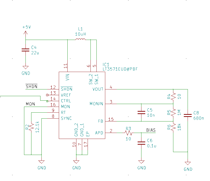
Here is my circuit diagram:

schematic

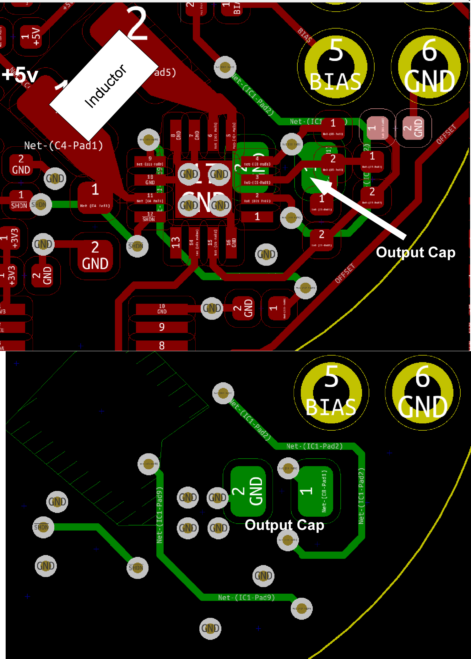
and here is the circuit layout:

layout

I apologize for the images, but the boost converter is stuck into a more complicated circuit with very little free area. I opted to put the output cap on the backside. This added vias but let me put the cap pad directly over the switching converter GND, so the loop area is very small. Most components are 0402. The board is 4 layers, with almost all components on the top, then GND, then PWR and finally the back signal layer which has the output cap. Should I have avoided the vias?

I tested with the current limiter set to 20mA and with it disabled and it made no difference.

My inductor is 10uH with < 350mOhm resistance and a saturation current of 1 amp. The converter is configured to run at 1 MHz. Not sure if these are ideal?

Any advice? I'm new to DC converters and not sure how to proceed.

Edit

I tested the power supply (0.07V total sag), and my decoupling seems fine (few 10s of mV p2p ripple under load measured at the device power pin).

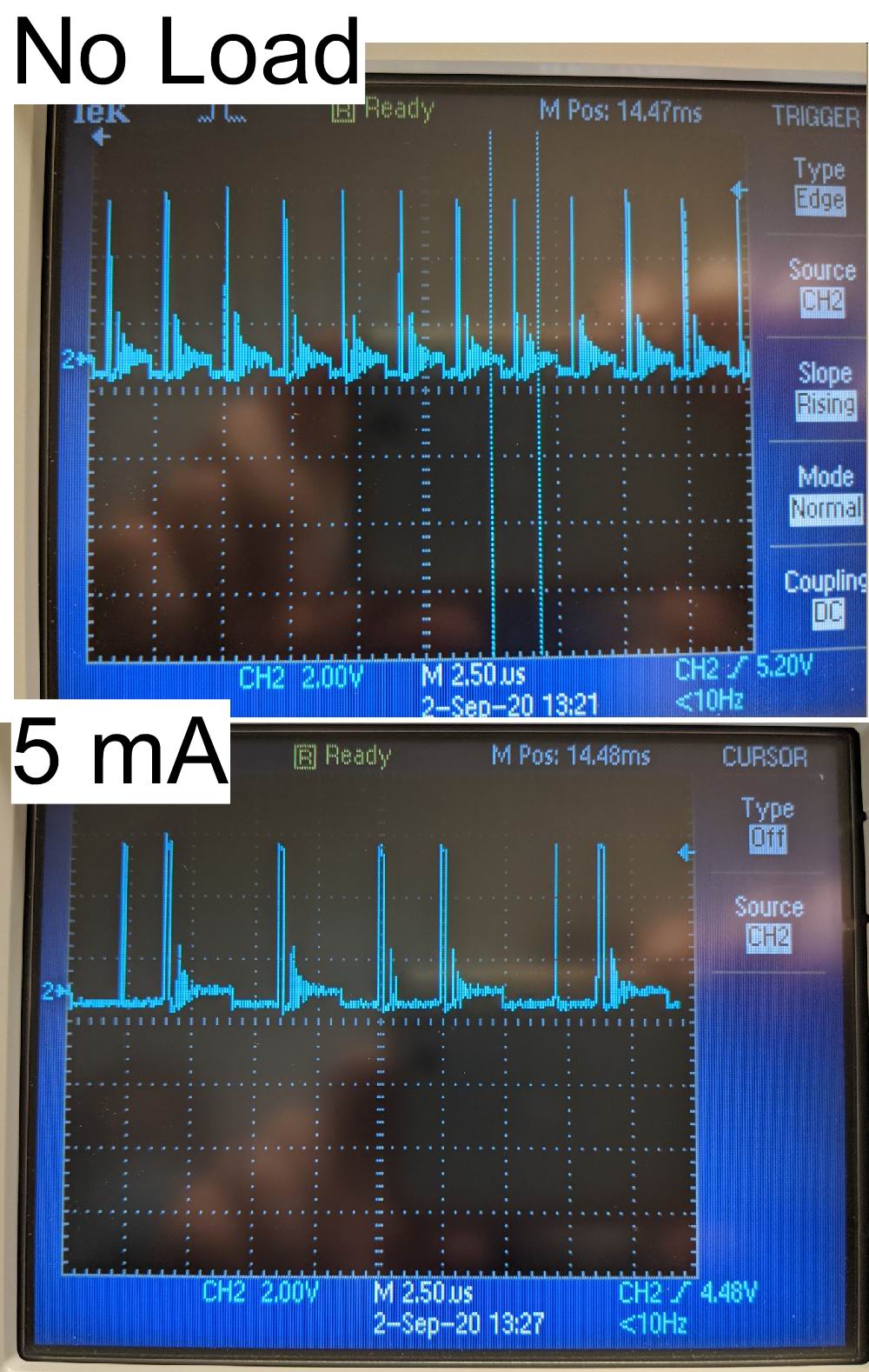
Following suggestions here, I tried lowering the switching frequency 2.2-fold (450 kHz) while increasing the inductor size an equal amount (22uH). Unfortunately, the voltage droop into 10kOHm was identical to my original 1MHz/10uH circuit (0.9V). I took a few simple measurements putting a scope probe on the switch/inductor trace (at 450 kHz/22uH):

switch voltage

Under load it seems the switching frequency becomes irregular, with some missing cycles, and a few that seem to happen too close together (?).

\$\endgroup\$
5
  • \$\begingroup\$ At 1 MHz the max duty cycle can be as low as 85%, maybe consider running at a lower switching frequency. \$\endgroup\$
    – John D
    Commented Aug 23, 2020 at 3:04
  • \$\begingroup\$ Use a smaller output cap 0.1uF=2 Ohms , 10uH is 50 Ohms at 1MHz \$\endgroup\$
    – D.A.S.
    Commented Aug 23, 2020 at 4:35
  • \$\begingroup\$ I notice that MON is grounded - is there a reason for this? Is your input 5 volt supply remaining stable when you take load current? \$\endgroup\$
    – Andy aka
    Commented Aug 23, 2020 at 8:34
  • \$\begingroup\$ @TonyStewartSunnyskyguyEE75 The answer below suggested a larger output cap, and intuitively I would have expected a smaller impedance to ground to at least not hurt. What is the downside of a large cap (aside from time to charge and inrush currents)? \$\endgroup\$ Commented Aug 24, 2020 at 1:33
  • \$\begingroup\$ @Andy aka I'll test if adding a resistance to the MON pin improves performance. Good catch. I believe the power remains stable (current is a small fraction of capacity), but that is a simple thing to verify so I will double check. \$\endgroup\$ Commented Aug 24, 2020 at 1:35

2 Answers 2

1
\$\begingroup\$

Following the advice here, I experimented with adjusting the frequency and inductance values and found that I could squeeze slightly more current out with optimized values. In addition, by taking the switch output directly and ignoring the APD pin I could also slightly reduce losses. Collectively these got 8mA with only a few hundred millivolts droop. Ultimately though this design is limited by the switch integrated into the device, but this was good enough for my purposes.

\$\endgroup\$
0
\$\begingroup\$

These chips seem to all operate in the same basic way . Hardswitching peak current mode . Things are not good for a boost at high boost ratios and things are not good for a buck at high stepdown ratios .Fortunately Linear tech have pinned out a RT pin that will allow you to reduce frequency .Increase R2 and L1 and C8 to get your product out the door . Many of these chips do not pin out frequency which is bad .The use of a diode pump can get you out of a hole if you must use the chip.

\$\endgroup\$

Your Answer

By clicking “Post Your Answer”, you agree to our terms of service and acknowledge you have read our privacy policy.

Not the answer you're looking for? Browse other questions tagged or ask your own question.