6
\$\begingroup\$

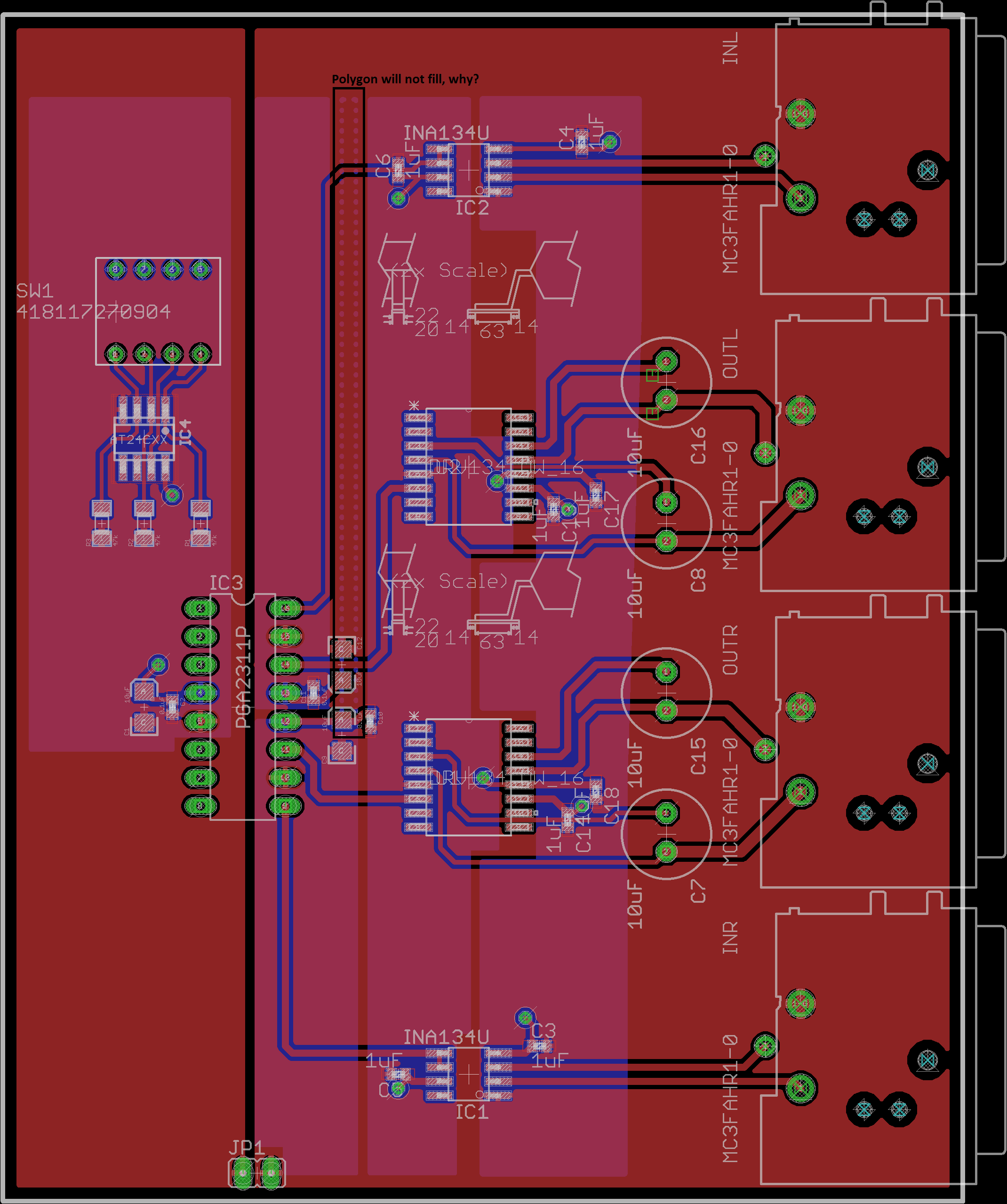
I am working on a volume control board using PGA2311 and this IC needs two GNDS - analog and digital. Why does the DGND polygon not fill? The image below shows the problem:

Polygon settings

Now I have similar problem, the polygon won't fill, any ideas? It is ANALOG +5V polygon.enter image description here

\$\endgroup\$
8
  • 1
    \$\begingroup\$ Did you make sure the fill is on the same net as the DGnd? Because it might not have the same name. \$\endgroup\$
    – Passerby
    Commented Jun 24, 2013 at 6:57
  • \$\begingroup\$ I did, I highlight DGND pin on IC and polygon gets highlighted, just won fill! \$\endgroup\$ Commented Jun 24, 2013 at 7:36
  • 1
    \$\begingroup\$ Maybe its a problem with your enclosing Dimension layer? From your picture, its not entirely clear where the outline is. Polygons outside of dimension won't fill. \$\endgroup\$
    – Rev
    Commented Jun 24, 2013 at 9:25
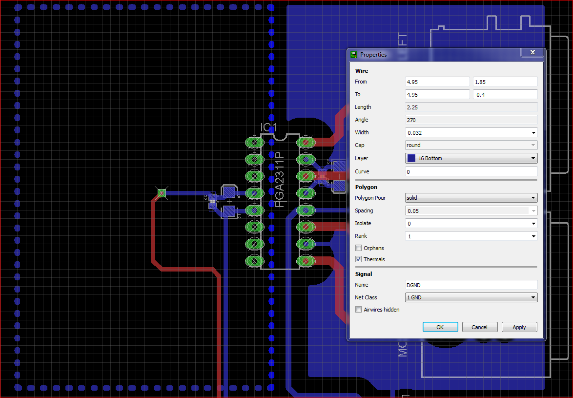
  • \$\begingroup\$ Here are two screenshots, first for Polygon Highlight (IC's pin DGND is connected to polygon) and the second one represents polygon info.PolygonInfo and HighlightedPolygon \$\endgroup\$ Commented Jun 24, 2013 at 11:47
  • 1
    \$\begingroup\$ Try running the ratsnest tool? For some reason this seems to be the trigger for updating of polygon fills. \$\endgroup\$ Commented Jun 24, 2013 at 18:41

1 Answer 1

4
\$\begingroup\$

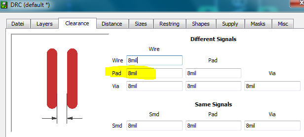
Looking at the clearance area around your pads, the problem is most likely the pad-to-wire clearance setting in your design rules. If the clearance (minimum distance) is set too high, the polygon place can't connect to the respective PIN. As a result, the polygon won't fill at all.

I can reproduce your problem just fine setting the highlighted value to something like 80 mil.
design rules

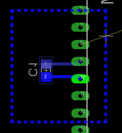
This polygon fills fine using a pad-to-wire clearance of 8 mil, but not 80 mil.
enter image description here

If that does not solve the problem, it may also be a restriction that you defined in your NET classes. So check those too.

EDIT:
Another idea to narrow down the problem: Got to the polygon settings and check the "Orphans" setting. This will instruct eagle to create polygons, even if there is no way to connected them. If this helps, its definitely the problem that your PAD can't be connected due to some limiting rule.

EDIT2:
As stated in the comments, orphaned polygons will be processed. So it comes down to one of these:

  • the wire width of the polygon is set too high
  • at least one of the relevant clearance values in the design rules is to large
  • at least one of the relevant clearance values in the net class specifications is to large
\$\endgroup\$
8
  • \$\begingroup\$ Setting clearance also does not help and in schematics I've setup both AGND and DGND as GROUND Net class. \$\endgroup\$ Commented Jun 25, 2013 at 6:27
  • 2
    \$\begingroup\$ Check that <Options -> Settings -> Misc: "ratsnest calculates polygons"> is selected. If you rip-up the "functioning" polygon and select ratsnest, will it properly fill again? \$\endgroup\$
    – Rev
    Commented Jun 25, 2013 at 6:42
  • \$\begingroup\$ That option is selected/turned ON. \$\endgroup\$ Commented Jun 25, 2013 at 6:50
  • \$\begingroup\$ Wow, trick with "Orphans" did the job, polygon fills now! But why DGND from IC's pin is not connected to polygon, nevertheless if I click with "Show" on GND, both pin and polygon get highlighted? \$\endgroup\$ Commented Jun 25, 2013 at 6:53
  • \$\begingroup\$ Glad to hear that, but you still have to fix it, since the GND polygon is obviously useless without connection. \$\endgroup\$
    – Rev
    Commented Jun 25, 2013 at 6:54

Your Answer

By clicking “Post Your Answer”, you agree to our terms of service and acknowledge you have read our privacy policy.

Not the answer you're looking for? Browse other questions tagged or ask your own question.