1
\$\begingroup\$

I have a circuit which includes two back-to-back switching regulators. The first is used to take the input of 14 V to 5 V and the second charges a 2-cell lithium battery.

I have verified the problem to be with the first regulator. I cut the connection between the Vout of the 14 V to 5 V regulator and supplied the second regulator with a constant 5 V and it worked as intended.

The problem with the 14 V to 5 V regulator seems to be instability and a changing nominal output voltage. At 6 V Vin the regulator is outputting something close to 5 V, but as the input voltage increases (even to just 14 V), so does the instability and the nominal output voltage increases above 6 V which is too high for my application.

The ICs on the output side are outputting overvoltage protection at about 6 V. On the instability, I see the output voltage on the oscope having +/- 0.7 V on the nominal output voltage. I have fried my IC during testing, but can solder a new one on here shortly.

Why would the nominal output voltage of this regulator potentially rise with input voltage? If I add more capacitance on the output voltage will it smooth the output signal and prevent these voltage fluctuations?

circuit

Datasheets:
RFN1LAM6STFTR
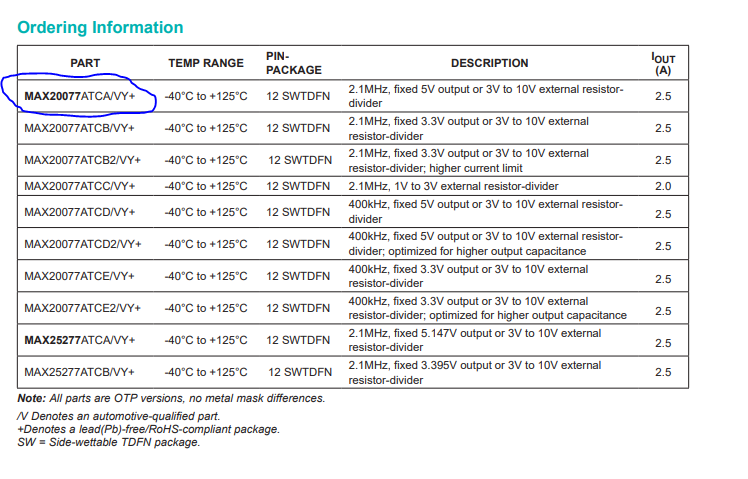
MAX20077ATCA_VY+
SF-1206SA150M-2
SRP3212-2R2M
865080340001
865230443003
CNC5L1X7R1C106K160AE

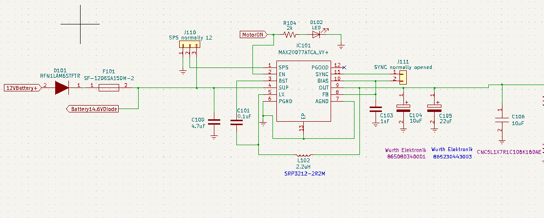
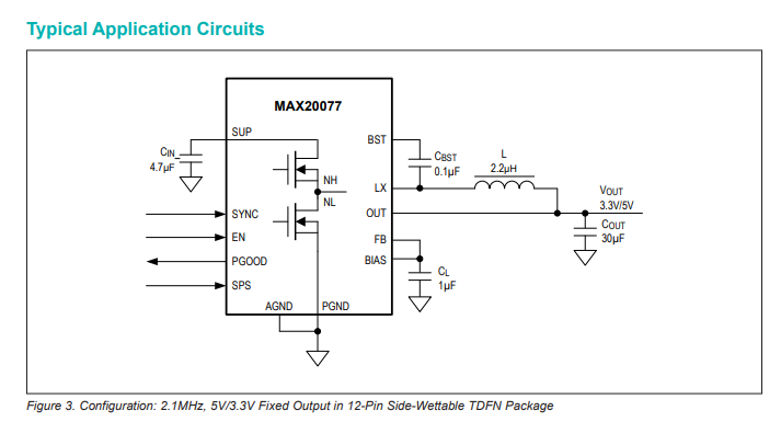
circuit from datasheet

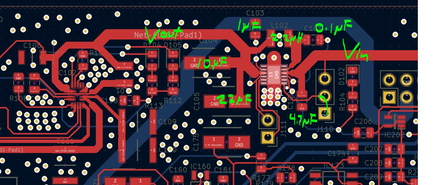
layout

regulator properties

\$\endgroup\$
18
  • \$\begingroup\$ My suspicion is that you aren't meeting the minimum ESR requirements on the output capacitor. What capacitors are you currently using on the outputs? Are they aluminium electrolytics, tantalums, or MLCCs? What're their voltage ratings? Do you have exact part numbers for them? \$\endgroup\$
    – Polynomial
    Commented Jan 30, 2023 at 14:54
  • \$\begingroup\$ @Polynomial interesting comment. I will add the mfr# of the capacitors. In general they are aluminum electrolytic on the output of the 1st switching regulator. But the 2nd regulator only has X7R ceramic capacitors as it was specified by the manufacturer. \$\endgroup\$
    – Feynman137
    Commented Jan 30, 2023 at 15:24
  • \$\begingroup\$ D101 is apparently called RFN1LAM6STF not 5TF. What diode did you end up mounting there? \$\endgroup\$
    – Lundin
    Commented Jan 30, 2023 at 15:27
  • 2
    \$\begingroup\$ Check if you have problems with ground bounce. It seems most likely to me that the problem is related to PCB layout, so show us a picture of that. An oscilloscope image of the voltage at the switch node would be nice as well. \$\endgroup\$
    – Hearth
    Commented Jan 30, 2023 at 16:08
  • 1
    \$\begingroup\$ Now that you've posted the layout, could you explain why there are no vias directly under the IC? I assume all the ones that are there are going directly to an internal ground plane (if not, that's probably your problem), but why put them all outside the IC instead of internal thermal vias? \$\endgroup\$
    – Hearth
    Commented Jan 30, 2023 at 16:42

1 Answer 1

2
\$\begingroup\$

I believe the culprit is the layout of the output node of the IC.

The OUT pin of this chip is really just a sense pin, that closes the loop with the control of the output voltage. The way you have connected it, there is a lot of common path between the OUT pin, and the output side of the inductor.

Imagine all the AC current that is flowing out of the inductor, into the output capacitors: the feedback pin is going to see lots of movement there, missing out on most of the smoothing effect of the caps, because you have hooked it more or less in the mid point.

A better layout would require the feedback signal to have a separate path, ideally connecting directly in the pad of one of the output caps, on a side where no AC current is expected.

It is very well possible that this effect is visible only above a certain input voltage because the duty cycle will be different, and the ripple current in the inductor will change.

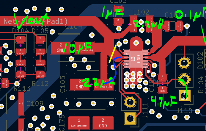
One thing you might be able to do to prove this is to cut the track from OUT to the caps, soldering a thin wire to it and connecting it on a location where no AC current is flowing, e.g. on the track going to your charger IC.

Here is the proposed cut: Proposed fix as described above

In Yellow the cut, in blue a wire going to the pad of a cap.

\$\endgroup\$
4
  • 1
    \$\begingroup\$ And by the way, the way they draw the example schematic on the datasheet is a bit misleading, in my opinion. \$\endgroup\$ Commented Jan 30, 2023 at 17:08
  • \$\begingroup\$ Would you mind drawing the proposed line cut onto the layout screenshot I attached? I am about 90% certain I understand what you are saying and will try this but I want to be sure. Also it would be interesting to see how far down you propose reconnecting the capacitors. \$\endgroup\$
    – Feynman137
    Commented Jan 30, 2023 at 18:32
  • \$\begingroup\$ Please see the edit. \$\endgroup\$ Commented Jan 31, 2023 at 9:06
  • \$\begingroup\$ After some testing and modification it is true changing the layout by cutting a trace and attaching a small wire will make this circuit function as intended. However the location of the necessary cut is slightly different then proposed on 1/30. See figure 3 (page 15) on the Max datasheet which shows the inductor loop close to the IC and the capacitors closer to the load. The C104 and C105 input trace should be cut and reattached to Vout near the top left of the footprint screenshot I attached. \$\endgroup\$
    – Feynman137
    Commented Feb 5, 2023 at 0:54

Your Answer

By clicking “Post Your Answer”, you agree to our terms of service and acknowledge you have read our privacy policy.

Not the answer you're looking for? Browse other questions tagged or ask your own question.