27
\$\begingroup\$

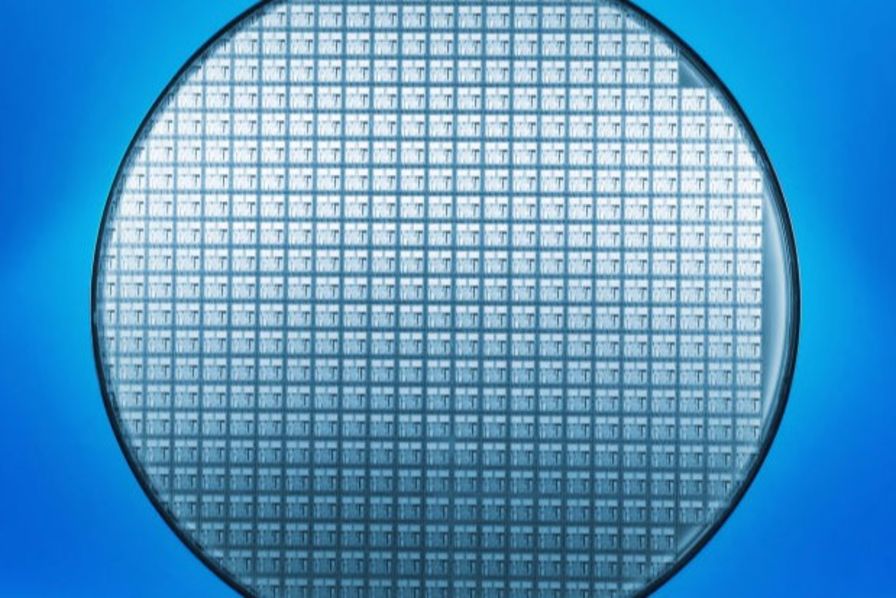
Around the edge of a wafer (see image below) you will observe that there are many partial dies. It seems wasteful to use the lithography machine to print these partial dies because they will be discarded later. Surely the stepper motors that move the wafer could be programmed to stop at only those locations where a full die fits on the wafer. By doing so they would use the lithography machine more efficiently.

Why do they instead print dies right up to the edges?

enter image description here

In this CNBC video, you can see how a modern lithography machine steps the wafer to image dice sequentially. (Note: I am not affiliated with CNBC or any company in the chip fabrication industry)

\$\endgroup\$
3
  • 1
    \$\begingroup\$ Maybe you can get some information on how to improve the process or yield out of the structures at the edge - that's just guessing... \$\endgroup\$
    – Arsenal
    Commented Dec 15, 2023 at 14:06
  • \$\begingroup\$ There are no stepper motors, only high end servo drives and stages. \$\endgroup\$
    – TQQQ
    Commented Dec 16, 2023 at 14:47
  • 1
    \$\begingroup\$ Just a guess, but theoretically it could affect the evenness of any chemical processing steps whether each chip is bordered by similar density of structure vs. unexposed photoresist. \$\endgroup\$
    – jpa
    Commented Dec 16, 2023 at 20:22

4 Answers 4

24
\$\begingroup\$

I'm not sure of all the reasons, but one reason is that the stepped field doesn't always contain just one die: you might have four dice in a 2×2 arrangement per field, and it's usually worth it to get the one extra die even if the other three are all cut off.

In the extreme, you have the situation used in the largest mass-production scenarios (at least at larger process nodes; I don't know anything about modern process nodes), where the entire wafer is imaged at once with a single mask with an entire wafer's worth of dice on it. In that case, there's no benefit (that I'm aware of, anyway) to having the single mask contain dice off the edge of the wafer, but there's no harm either--you still only image the wafer a single time per mask, so it's not like you're adding extra time under the stepper.

And finally: They don't always! One of the fabs my workplace gets wafers made at doesn't image all the way to the edge; even when a field would have some full dice on it, if it's off the wafer edge, it's left off. This might just be because it's an experimental process, though (the device we're making is something weird that needs a custom process), and yield is already low enough (for the moment; we're working on that) that most of the dice closest to the edge are non-functional anyway, so ones even closer would definitely not work.

\$\endgroup\$
9
  • 3
    \$\begingroup\$ Edge effects are part of the picture in some cases. The edge of a wafer dissipates quite differently than the center, as I'm sure you can imagine. At G-squared with their still-research RTP (rapid thermal processing) back in the early 1990's -- a single-wafer unit designed to complete a wafer in a couple of weeks rather than several months required for boats of wafers -- used heating rates of 3-5 C per second. Wafers would "potato-chip" due to uneven heating related mostly to that edge effect. That issue was why Chris Gronet (CEO/physicist) invited me to CA. Nice answer. +1 \$\endgroup\$ Commented Dec 15, 2023 at 6:42
  • 2
    \$\begingroup\$ Could something like this potato-chip problem be the real reason? If so, it might deserve to be embellished in an answer. \$\endgroup\$
    – phil1008
    Commented Dec 15, 2023 at 8:01
  • 1
    \$\begingroup\$ @phil1008 If you don't include my name, I don't get messaged. I didn't discussed that choice with the FAB engineers. But an educated guess would be that if they didn't include the dice out to the edge, then there would be an impact to heat dissipation at the newly exposed outside dice perimeters. So yes, I have some reason to imagine this could very well be why, at least until they had evidence to the contrary, they would choose to avoid the issue entirely and simply keep the pattern going all the way to the edge. \$\endgroup\$ Commented Dec 15, 2023 at 8:16
  • 3
    \$\begingroup\$ @phil1008 But my focus at the time was on issues of the lamp-heated environment and how to observe temps, non-contact, so that closed loop controls could control 100s of lamps to keep the surface evenly heated. So I can really only speculate. (I was able to see a solution in just a few hours' listening to Chris. Not because I'm smarter. Only because he was buried in the trees. As soon as I told him what I was thinking, he was immediately "yes, that'll work!" and "I'm drilling holes tonight. I'll let you know in the AM!" And he did! It worked! Cool experience for me. And good for him, too. \$\endgroup\$ Commented Dec 15, 2023 at 8:25
  • 1
    \$\begingroup\$ @phil1008 Hopefully, perhaps this gives you an additional story to use as good segue when asking an expert, someday in the future, who may be able to then give you an informed and comprehensive answer that includes whether or not this has anything to do with why. Or you could just call up Applied Materials and ask them. (I've done as much, myself, when curious. Just a cold call.) They might enjoy putting you in touch with someone there. If you are really curious, I think it would be worth the attempt. And you might get to know someone worthwhile knowing, too! \$\endgroup\$ Commented Dec 15, 2023 at 8:31
20
\$\begingroup\$

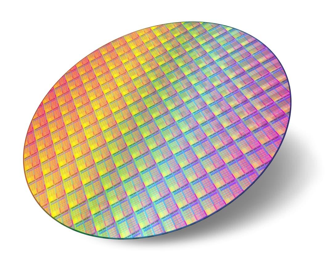
Put simply, the reticle has hundreds of copies of the die on it, and the reticle is a standard size for both big and small die sizes, meaning it would be more work to avoid doing photolith on the edges than to blindly do it.

This goes for all process layers, from doping to metallization. Edge dies are made simply because it would be more complicated not to.

Edit: I am an integrated circuit designer, and in college I worked in the photolith department of an IC fab. The last thing we do after design/layout/verification and before sending our reticles off to be manufactured is a final layer-by-layer visual inspection of the reticle, which contains huge arrays of the die at a fixed total size. The reticles are a fixed size, the photolith magnification is a fixed size, and so the photolith machines take a fixed amount of time to process a single wafer.

For a very big die size, you get more edge based yield loss. This is true for smaller wafers as well. Until they come out with a square silicon wafer, the best you can do is keep your die size small relative to your wafer size, at least in your production environment.

Edit 2: to expand on "Edge dies are made simply because it would be more complicated not to", I mean that if you did not step your reticle so it went all the way to the corner, you would either need to change your step pattern to avoid the corners entirely and suffer yield loss from the complete dies that would have been made from the inside corners of those reticles, or else design custom reticles that you had to swap in when you got to the edges of the wafer. The marginal cost of stepping a few extra fields is almost nothing (maybe a couple seconds total on the lith machine), and in general it gives you extra units, especially for small die size parts.

\$\endgroup\$
6
  • 3
    \$\begingroup\$ I'm having a hard time reconciling this answer with what I observe in this video: youtu.be/iSVHp6CAyQ8?t=266. It looks like the photomask is imaged once per die (or perhaps once per 2x2 patch of dies) in the video. Can you elaborate and perhaps provide sources for your information? \$\endgroup\$
    – phil1008
    Commented Dec 15, 2023 at 7:45
  • 2
    \$\begingroup\$ @phil1008 this is first hand information from working in the field, both in design and fab. See my edit \$\endgroup\$ Commented Dec 15, 2023 at 16:23
  • 1
    \$\begingroup\$ How long ago was college? For leading edge chips now, the maximum chip size is reduced from what it used to be. \$\endgroup\$
    – Jon Custer
    Commented Dec 15, 2023 at 19:43
  • \$\begingroup\$ Can you add a source for "the reticle has hundreds of copies of the die on it"? I'm worried that this is inaccurate based on my knowledge of the industry - which I admit is far from perfect. The statement "Edge dies are made simply because it would be more complicated not to." does not seem like a very satisfactory answer. For people who upvoted, can you add a comment to explain what you liked about this answer to help mapplejacks out? \$\endgroup\$
    – phil1008
    Commented Dec 15, 2023 at 21:32
  • 3
    \$\begingroup\$ @phil1008 my source is, I design ICs, and I have looked at the reticles, both in software and physically. For the processes I have worked with (90nm, 180nm), this is true. Some of my parts have >10k units yield per wafer. This would not be the case for huge dies, e.g. multicore CPUs, especially on small wafers. \$\endgroup\$ Commented Dec 15, 2023 at 22:15
8
\$\begingroup\$

The explanation in this answer is plausible: a rectangle with the image of several chips is imaged at a time. A step is made if any chip imaged in the step would be fully on the wafer, very often resulting in chips partially on the wafer.

It's only when a step would contain no chip fully on the wafer that it is left an un-etched wafer area. This happens, but only rarely if the imaging area is large. The photo below is adequately explained if it's imaged 3 chips horizontally at at time, and 2 or 4 vertically (the right 3 columns are 16 chips high) radiofrequency ICs from Somos Source: Somos press communication


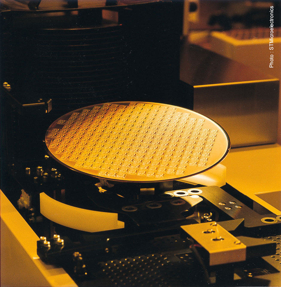
However that explanation does not seem to apply for the following picture, where the number of chips horizontally must divide 3 and 2, thus must be 1; and must be 1 vertically too.

ST Microelectronics SE2 Source: ST Microelectronics press material

\$\endgroup\$
2
  • 1
    \$\begingroup\$ This is a good complement to my answer, but bear in mind that any images you add need to have mention of their source! If you took the pictures yourself (or got them from a coworker, or some other offline source), you can say as much, but if you found them online give a link to where you found them. \$\endgroup\$
    – Hearth
    Commented Dec 16, 2023 at 13:44
  • 1
    \$\begingroup\$ @Heart: Good reminder. I hope I'm fine now. \$\endgroup\$
    – fgrieu
    Commented Dec 16, 2023 at 14:25
1
\$\begingroup\$

Imagine a sheet of paper on which you want to print multiple copies of a picture:

You could cut the paper into squares to fit the picture perfectly, but you'd waste some paper. Printing the picture right up to the edges might seem wasteful too, but it uses the paper more efficiently. Similarly, in semiconductor manufacturing, maximizing wafer utilization is crucial for cost-effectiveness, even if it means printing some partial dies.


Circular wafers are the standard in the industry due to their efficient use of silicon material. Cutting the wafer into squares before printing the dies would leave significant unused silicon at the corners, increasing waste. Some semiconductor fabrication processes can be sensitive to the pattern density around the die. Printing partial dies creates a buffer zone, mitigating these edge effects and ensuring consistent quality for the usable dies.

\$\endgroup\$
3
  • 4
    \$\begingroup\$ I think circular wafers are the standard not because of any increased efficiency, but just because a lot of the processing steps (such as spin coating, which is done several times throughout the processing of a wafer) rely on them being circular or just work best on circular wafers, which in turn happened because circular wafers are easiest to make. Circular is what you naturally get by slicing up a boule grown by the Czochralski process (which I think is no longer the method used to make wafers, but it was when these standards were being decided on). \$\endgroup\$
    – Hearth
    Commented Dec 15, 2023 at 18:53
  • \$\begingroup\$ Base Si wafers are still grown by Czochralski, but may well have further processing for the silicon-on-insulator top levels. The majority of the wafer is for mechanical strength, where the carbon content is important. \$\endgroup\$
    – Jon Custer
    Commented Dec 15, 2023 at 19:46
  • 1
    \$\begingroup\$ @Hearth you're right, and another consideration is vignetting for many steps (like metal deposition). These processes are radially symmetrical. If you design a process step so that it could reach all the way to the corners of a square wafer and have satisfactory results on the corners, then you may as well put a round wafer in there with ✓2 times your original diameter. \$\endgroup\$ Commented Dec 15, 2023 at 23:01

Your Answer

By clicking “Post Your Answer”, you agree to our terms of service and acknowledge you have read our privacy policy.

Not the answer you're looking for? Browse other questions tagged or ask your own question.