2
\$\begingroup\$

I'm trying to drive a PWM controlled 12V light (specifically, an inverter which drives the light) with the pictured circuit.

The PWM is generated via a Raspberry Pi Zero 2 W. The BTS6143 (datasheet) should serve as the power switch, with the transistor connected to GPIO18 on the Pi controlling whether the switch is opened or closed.

When measuring the switch's output voltage, I always get around 6V, regardless of the transistor's state. I can see the transistor is having some effect: the voltage will change from about 6V to about 6.2V and back. I need this to cycle between the full 12V and 0V.

Without the light connected, the output voltage cycles between about 11.4V and 10.8V.

Measuring the voltages at the BTS6143's IN pin, I can see that it is properly being cycled between 0V and 12V. My understanding from the datasheet is that should mean the switch is either opened or closed, so the the output should be either 0V or 12V.

This is based off some instructions I found online, but that used an Arduino, in case that makes any big difference. I assume that means at least the basics of the circuit are sound.

In testing, I tried a couple additional things not shown in the diagram: shorting the BTS6143's two output pins as recommended in the datasheet, and putting a pull-up resistor between the 12V supply and the BTS6143's IN pin. Both of these made no difference.

Does anyone have any ideas on what's causing this to output the unexpected voltages? What is my misunderstanding of the BTS6143?

Circuit diagram

Edit with more pictures and details:

J3 is at the moment connected to nothing. Ultimately it'll be a PWM controlled servo, but I've just been focused on troubleshooting the 12V PWM out first (the PWM_OUT and PWM_OUT_BLK on the right of the diagram.)

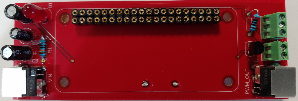
Top side of board

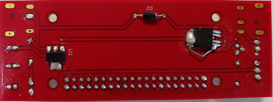
Bottom side of board

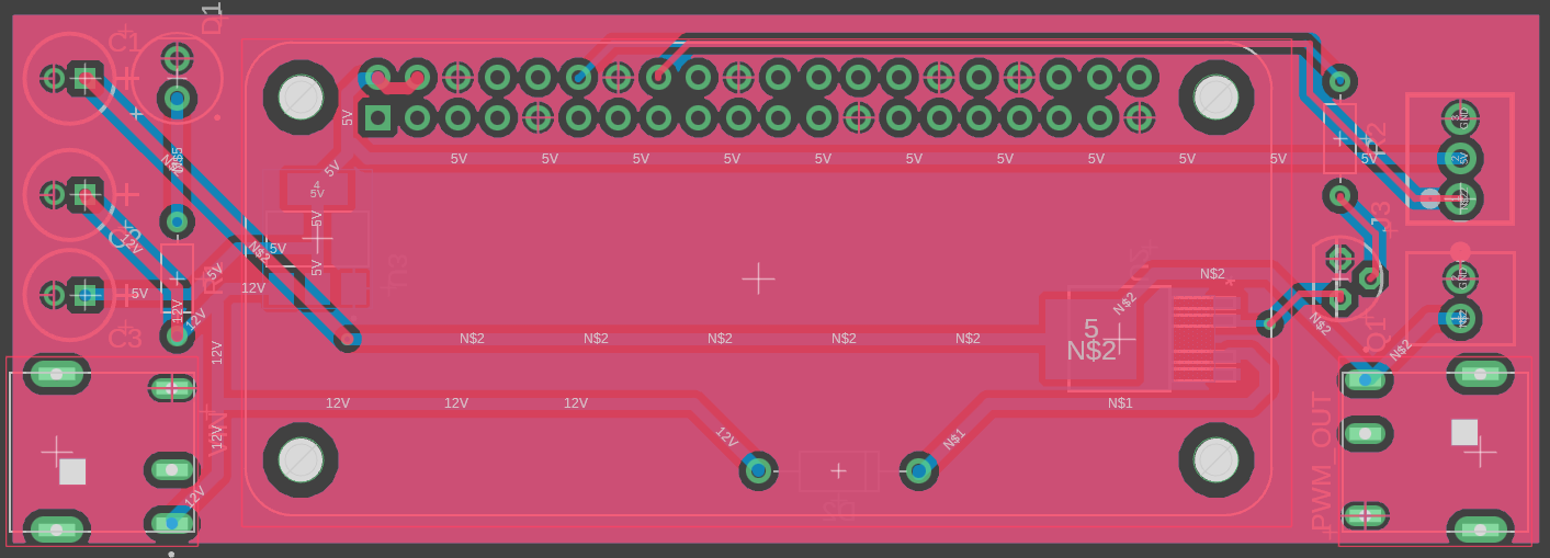
Top side of board design

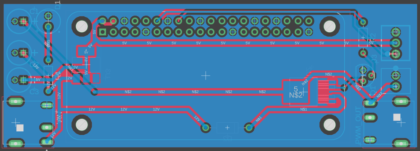
Bottom side of board design

\$\endgroup\$
11
  • 1
    \$\begingroup\$ What is J3 connected to? Can we see photos of the completed circuit (both sides of the board)? \$\endgroup\$
    – pion
    Commented Aug 28 at 19:35
  • \$\begingroup\$ J3 is at the moment connected to nothing. Ultimately it'll be a PWM controlled servo, but I've just been focused on trouble shooting the 12V PWM out first. I've updated the post with pictures. Thanks! \$\endgroup\$
    – ceej12
    Commented Aug 28 at 20:39
  • 1
    \$\begingroup\$ Just as an experiment, can you (1) detach the light from the inverter, (2) desolder Q1, (3) measure output voltage in that state (floating IN pin of the BTS6143) and then (4) connect a bare wire from the IN pin to ground and measure the output voltage? I.e. let’s just bypass the transistor entirely and try forcing the switch to either full low or floating. \$\endgroup\$
    – pion
    Commented Aug 28 at 21:51
  • 1
    \$\begingroup\$ If you want to see a voltage at U2 OUT (pins 1&5 OUT) switch between high and low voltage, you need to apply a current sinking load between those pins and ground, such as a 1K Ohm 1/4Watt (or higher wattage) resistor. The U2 is a HIGH-SIDE SWITCH, so when not activated (which occurs when U2 IN is open/floating) the U2 OUT pins will be Floating. A volt meter is too high impedance to overcome internal parasitic leakages of U2 and bring the output voltage to zero. With your normal load (outside the schematic) removed, instead attach a 1K Ohm resistor to ground and then measure again. \$\endgroup\$
    – BK303
    Commented Aug 29 at 2:57
  • 1
    \$\begingroup\$ Also, when first testing the circuit, be sure to drive the GPIO control output statically or very slow switching between high/low (maybe 1 second high, 1 second low). The U2 (BTS6143) is a very high-current switch with relatively long turn on/off time of 500 µs (max). So during normal operation, the GPIO control signal when operated as PWM should limit frequency to bellow about 1/(20 * 500 µs) = 100Hz for 5% control precision, so that the on/off durations are each always longer than 500 µs. \$\endgroup\$
    – BK303
    Commented Aug 29 at 3:19

1 Answer 1

5
\$\begingroup\$

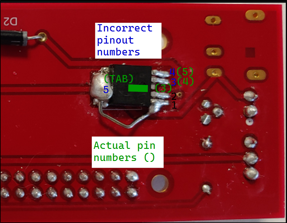
Missed it on first glance, but I believe the problem is that you designed with the wrong footprint pinout numbers for the BTS 6143 D (U2). Your design was assuming the footprint pin numbers I marked below on your photo in blue, but the correct footprint pin numbers for pins 3-5 I've marked in green. Pin 1,2 were correctly numbered. The bottom pad/tab is internally connected to pin 3 (my dark green bar), which is why pin 3 is cut short and not connected to the PCB. Bummer the Infineon datasheet is very unclear on the pin numbering, but this pin numbering is basically by convention and was not explicitly labelled. I couldn't even confirm the pin numbering on the package page downloads for that PG-TO252-5-11 case, but I'm confident that I'm correct and the green pin numbers are good package design sense (tab/3 is input, end pins 1/5 are output). If you have one of the ECAD package on this page, you can download their official symbol/footprint and double check. Or easier, take a spare part and verify internal continuity between the cut pin 3 and the bottom pad/tab, and internal continuity between pins 1 and 5. marked up photo with cut pin #3 and tab labeled

Another issue, which you mentioned in your last comment, is that C1 (100µF) should not be included on the OUT net, which is not appropriate if you plan to PWM switch the output. Also, reconsider why was D2 included, which is just acting as a heater if the load can't source power and needs to be sized to carry full load current.

By the way, what is your intended maximum load current? The BTS 6143 D can handle 10A and higher under certain conditions, but the amount of copper you have on in layout traces from Vin, through D2, and to VBatt, and then after U2 to the output connector seems far to small for 10 Amps or above.

\$\endgroup\$
5
  • 1
    \$\begingroup\$ note, added to answer a method to verify pinout with spare part by continuity checks (pins 3-to-Tab and then pins 1-to-5). Just want to make sure @ceej12 is aware of that late hint. \$\endgroup\$
    – BK303
    Commented Aug 29 at 5:23
  • \$\begingroup\$ Yep, you were right. The pins had continuity as you expected. I de-soldered the BTS6143, cut the traces, and routed things manually and it now works, properly blinking the light! So much for "Built & Verified by Ultra Librarian." Thanks for your help! \$\endgroup\$
    – ceej12
    Commented Aug 29 at 14:48
  • \$\begingroup\$ As for your other questions/comments, the diode D2 was in the original design, so I'm not certain, but I think it's to prevent powering things if you were to plug the power cable into the wrong place (PWM_OUT). That way the on-board LED would only light if the power was in the right plug. Under normal operation, would it be a problem? \$\endgroup\$
    – ceej12
    Commented Aug 29 at 14:53
  • \$\begingroup\$ And for max current, the light panel should only use a max of 250mA, and the Pi shouldn't be using much either. I used Digikey's trace calculator to size them, but I had to guess on some of the values. Do you think they're properly sizes for <500mA? Thanks for everyone's help! \$\endgroup\$
    – ceej12
    Commented Aug 29 at 14:58
  • \$\begingroup\$ the existing traces look appropriate for 250 to 500mA, and it's common to expand power traces or planes to use up more space at end of layout during cleanup to minimize power loss. I don't think D2 is going to help, as the U2 power switch would already stop back-current from entering the microprocessor (and power LED) if a power source was accidentally connected to the output instead of input. Advised protection is to add zener diode or transient voltage suppressor (TVS) with voltage rating a little higher than the maximum input voltage back-biased onto the Vout rail (where C1 was). \$\endgroup\$
    – BK303
    Commented Aug 31 at 2:29

Your Answer

By clicking “Post Your Answer”, you agree to our terms of service and acknowledge you have read our privacy policy.

Not the answer you're looking for? Browse other questions tagged or ask your own question.