20
\$\begingroup\$

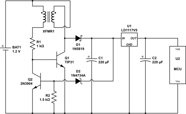
Please explain to me why this circuit can give me a regulated 5 V? I understand the Joule Thief part, but why the regulator part work?

schematic

simulate this circuit – Schematic created using CircuitLab

Especially, why the Zener diode D2 is crucial at preventing the 1117 and the MCU from being fried, and why the cap C1 should not be fully charged at all times?

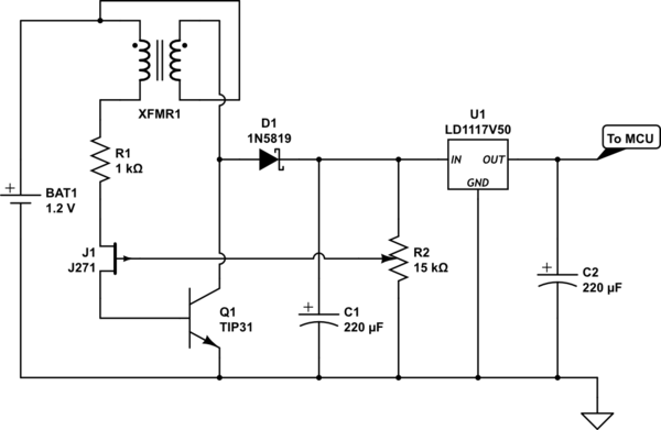
Since you all are suggesting a closed loop design, does this look better? (Remind you that the MCU won't take a pulsing power rail too well so I just keep the LDO there with as little headroom as possible to achieve proper regulation.)

schematic

simulate this circuit

The above schematic is modified to include the resistor Olin suggested.

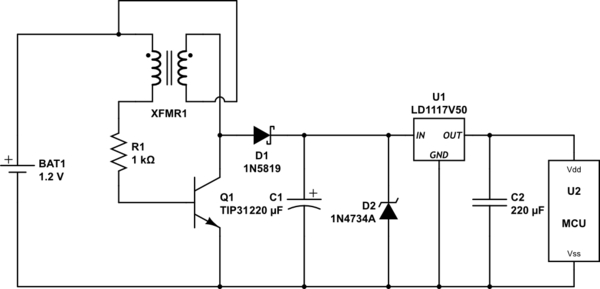
Will this work with less loss?

schematic

simulate this circuit

Tweak R2 in this schematic so that JFET pinches off when the voltage across C1 goes above 6 V (enough headroom for 1117 here.)

\$\endgroup\$
1
  • 1
    \$\begingroup\$ For further improving your question with all the feedback already you deserve +1 \$\endgroup\$
    – jippie
    Commented Jan 30, 2015 at 18:25

2 Answers 2

13
\$\begingroup\$

That's a pretty crappy circuit. Note that the boost converter is running completely open loop. There is no feedback that shuts it down when its output gets high enough. You don't show what the voltages of the zener and the linear regulator are, but most likely the zener is there just to make sure the input doesn't get above what the cap and the linear regulator can handle. The linear regulator then produces the nice and steady output voltage.

The reason I say this is a crappy circuit is because it is quite wasteful. That's usually a bad thing when running from a battery. Instead of adding feedback to the boost switcher, the extra power just gets wasted in the zener and the linear regulator. It would only take one more transistor to turn on when the regulator has a bit more voltage than it really needs. This transistor would kill the oscillations of Q1, thereby shutting down the boost converter until the voltage dropped again. This is essentially adding some loose regulation to the switcher output.

Added:

I see from the comments that there is interest in discussing how to regulate the switcher so that it's not running open loop.

As Russell and I both mention, in this case a NPN transistor that pulls the base of Q1 low is one means to kill the oscillations. Now the problem becomes turning on this transistor when the switcher output gets high enough. In the context of this circuit, as Russell has already mentioned, the simplest way is to have the bottom of the zener go into the base of this second oscillation-killing transistor. I'd also put a resistor from that base to ground to make sure this transistor doesn't come on just due to leakage. When the switcher output gets high enough, the zener conducts, which turns on the new transistor, which kills the oscillations so that the switcher stops making high voltage until that voltage goes a little lower again.

A totally different way to get a "voltage is high enough" signal is what Russell alluded to in a comment. This is putting a PNP transistor around the regulator such that it turns on when the input of the regulator is the B-E drop of the transistor above the regulator output. That threshold-detecting transistor would then be used to turn on the oscillation-killling transistor. I go into more detail about this method of threshold detecting as feedback to a switcher at https://electronics.stackexchange.com/a/149990/4512.

Added 2:

I see you have now added a updated schematic. Yes, that's exactly what Russell and I are talking about.

I would only make a small refinement by adding a resistor from the base of Q2 to ground. This guarantees some minimum current thru D2 before the switcher is shut down. If you don't do this, the voltage across D2 could be significantly less than its zener rating. Look at the datasheet for D2. It's voltage will be guaranteed only above some minimum current. Without knowing anything about that zener, I'd aim for about 500 µA. Figure the Q2 base voltage will be 600 mV, so that make the resistor 1.2 kΩ.

\$\endgroup\$
10
  • 1
    \$\begingroup\$ Just out of curiosity, where would this transistor be placed? \$\endgroup\$ Commented Jan 30, 2015 at 16:49
  • \$\begingroup\$ eg put an NPN with base "under" D2 so that when D2 conducts the transistor turns on. Emitter to ground and collector to base of Q1. When Vout is about 6V the converter base drive will be shunted. \$\endgroup\$
    – Russell McMahon
    Commented Jan 30, 2015 at 16:51
  • \$\begingroup\$ @Ignac: There are various ways this could work. My first knee-jerk reaction is to put C-E between the B-E of Q1. When that second transistor turns on, Q1 is held off, which would kill the oscillations and therefore stop making high voltage. That would still waste some power thru R1, and you'd have to make sure oscillations start up again when this feedback transistor turns off. There are other ways too, like using a FET instead to open the connection to the battery. \$\endgroup\$ Commented Jan 30, 2015 at 16:53
  • \$\begingroup\$ A "nice" alternative is to place a transistor across U1 input-output so that when the regulator gets about 0.6V headroom the transistor turns on. this can be NPN with emitter at Vout and base at Vin (via a resistor or a PNP the other way round. You then use it to affect the oscillator in some way. I did this long ago and moved the oscillator mark-space ratio and got a very smooth linear control of regulator action. Olin long ago also noted having done similar - we both arrived at the iea independently. My osillator was a 74C14 Schmitt trigger inverter - allowing a low cost and effective SMPS \$\endgroup\$
    – Russell McMahon
    Commented Jan 30, 2015 at 16:55
  • \$\begingroup\$ - Ransistor across U1 can supply > 0.6V headroom if needed. \$\endgroup\$
    – Russell McMahon
    Commented Jan 30, 2015 at 16:58
10
\$\begingroup\$

Can you post a link to where you got the claims from. The comment re C1 does not make full sense.

JT (Joule thief) circuits are usually poorly designed or not really designed or show signs that the people who produced them did not have a good understanding of what they were doing. This circuit is in that class.

The LD1117 has a maximum input voltage of 15V. Higher than that will kill it.
LM1117 data sheet The zener diode is meant to protect the regulator BUT it's voltage rating is lower than it should be.

The 1N4734A is a 5.6V 1 Watt zener. The zener voltage is too low to allow the LM1117 regulator to have adequate headroom at full current. It's likely that the "Joule thief" will not make enough power to let the LM1117 reach full rated output current.

The JT runs "openloop". If it makes more than 1 Watt it will try to destroy the zener and then the regulator and then the mcu. Without the zener, because the JT is a flyback converter the output voltage will ise until the energy available is dissipated. If the load is not accepting the available energy then the voltage keeps rising until the LM1117 starts to accept energy unintentionally (ie Vin_max exceeded).

Th C1 question's meaning is unclear. C1 may be fully charged without harm providing the voltages involved do not exceed the rated value os other connected components.

Overall this is not a good circuit. There are substantially better circuits available that do not depend on brute force dissipation of the converter output. Also, this circuit is not especially "designable" - it is difficult to say what the performance of the converter will be wrt power level or efficiency (but both are probably small).


Added 2022: My comment that better circuits were available was (very reasonably) queried in 2022 by @MicroservicesOnDDD

The OP's added second circuit is better as it provides feedback.
His 3rd circuit may be but is FET Vgson dependant.

A converter with more formal hysteresis turn on/off for the oscillator is liable to be more efficient.
If lowest cost or IC free designs are not a requirement then there are various ICs available that are able to be more efficient because they can address switching and regulation more properly.

An example only IC that addresses low power low-startup voltage applications is the LT3105. This is very expensive and while not ideal in performance, presumably represents state of the art when introduced. Datasheet dated 2019 - prior to that it was an Analog Devices product.

I don't know how the Joule Thief circuit's performance compares but it would be interesting to see as I'd class the 3105's performance as poor if it were not for the very low startup voltage.

https://www.analog.com/media/en/technical-documentation/data-sheets/3105fb.pdf
\$\endgroup\$
5
  • 2
    \$\begingroup\$ Maybe I need a higher rated Zener to protect the inputs. However can you tell me how to control it closed loop (I can use the MCU to mind this if the circuit can bootstrap itself, i.e. start open loop and when the MCU boots it becomes closed loop) \$\endgroup\$ Commented Jan 30, 2015 at 16:53
  • 1
    \$\begingroup\$ Also I would keep the LDO in there as, at least, some local regulation as the MCU won't take a pulsing power rail too well. \$\endgroup\$ Commented Jan 30, 2015 at 16:59
  • \$\begingroup\$ I don't understand "wrt" -- You said, "There are substantially better circuits available that do not depend on brute force dissipation of the converter output. Also, this circuit is not especially "designable" - it is difficult to say what the performance of the converter will be wrt power level or efficiency (but both are probably small)." Also, Would you please give us one of those "better circuits"? Thanks ahead of time, Russel! \$\endgroup\$ Commented Mar 19, 2022 at 14:01
  • \$\begingroup\$ @MicroservicesOnDDD wrt = with respect to. Sorry for lack of clarity. || His second circuit is better as it provides feedback. His 3rd circuit may be but is FET Vgson dependant. || A converter with more formal hysteresis turn on/off for the oscillator is liable to be more efficient. || If lowest cost or IC free designs are not a requirement then there are various ICs available that are able to be more efficient because they can address switching and regulation more properly. \$\endgroup\$
    – Russell McMahon
    Commented Mar 22, 2022 at 5:59
  • \$\begingroup\$ @MicroservicesOnDDD An IC that addresses low power low-startup voltage applications is the LT3105. This is expensive and while not ideal in performance, presumably represents stat of the art when introduced. Datasheet dated 2019 - prior to that it was an Analog Devices product. I don't know how the Joule Thief circuit's performance compares but it would be interesting to see as I'd class the 3105's performance as poor if it were not for the very low startup voltage. analog.com/media/en/technical-documentation/data-sheets/… \$\endgroup\$
    – Russell McMahon
    Commented Mar 22, 2022 at 6:16

Your Answer

By clicking “Post Your Answer”, you agree to our terms of service and acknowledge you have read our privacy policy.

Not the answer you're looking for? Browse other questions tagged or ask your own question.