3
\$\begingroup\$

I'm doing a high side switching of 5V 2A load and will be ON or OFF for long time(1-10 hours).

Now I'm confused about which transistors should I use ? or MOSFETs ? Do I need heatsink ? I really prefer SMD transistor or MOSFET, if its possible ?

I also want 5V on other side of transistor/MOSFET too. I'm sure there will be voltage drop, is there any way to get back the voltage drop ? First I thought to use bit high voltage in switching like 7V then put voltage regulator on other side so I can get right 5V. But since the load is 2A. The power will be 10W if I'm not wrong. Then I think its too much heat.

enter image description here

\$\endgroup\$
7
  • 1
    \$\begingroup\$ Power dissipation is voltage drop times current. If you use a mosfet with low enough \$R_{DS(on)}\$ then you can have a rather low drop. No drop is not possible, and likely not needed. \$\endgroup\$
    – PlasmaHH
    Commented Mar 24, 2015 at 15:58
  • \$\begingroup\$ For 2A, most certainly use a MOSFET. You can swap out the PNP for a P channel FET but get rid of R2 . Make sure the P-FET gate drive voltage is logic level. \$\endgroup\$
    – KyranF
    Commented Mar 24, 2015 at 15:59
  • \$\begingroup\$ what about fairchildsemi.com/datasheets/FD/FDN306P.pdf \$\endgroup\$
    – xmen
    Commented Mar 24, 2015 at 16:03
  • \$\begingroup\$ Its RDS(on) is 40 mΩ, means 0.08V drop. Making it 4.92V. Right ? \$\endgroup\$
    – xmen
    Commented Mar 24, 2015 at 16:05
  • 1
    \$\begingroup\$ @sherrellbc because of voltage drop. If you have plenty of voltage headroom you can use all the fancy 30A Darlington drivers you want, but at the cost of dropping 1+V and having to deal with the resultant power dissipation and large package sizes. \$\endgroup\$
    – KyranF
    Commented Mar 24, 2015 at 18:01

2 Answers 2

4
\$\begingroup\$

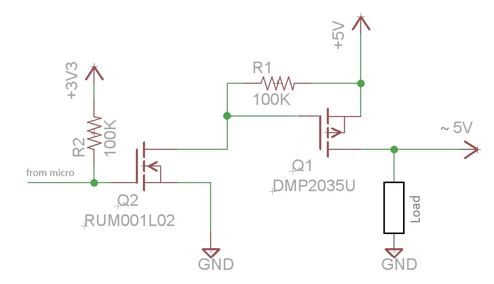
Like the BJT high-side switch shown in your question, this does the same thing using an N-channel and P-channel MOSFET:

enter image description here

If your microcontroller can tolerate 5 volts on its output pins, then you could hook up the output directly to the gate of the P-channel MOSFET in an open-drain configuration, and not need the N-channel device.

R1 is there to insure the MOSFET is on when the N-channel MOSFET is off. Because of the inverting nature of the N-channel MOSFET, a 0 on the output of the microcontroller turns on the load, and 1 turns it off. Adding a pull-up (R2) to 3.3v on the output of the microcontroller keeps the load off when the circuit first comes up. You will want to configure the microcontroller's output pin as open-drain.

Note there are no resistors in the gate circuits of the FETs, this is because they are voltage-driven devices unlike BJT's whose bases are current-driven.

The DMP2035U has a typical Rds(on) of 23 mΩ and can handle 2.9A continuous, and dissipate 0.8W. So the voltage drop will be about 45 mV, or about 4.95v across the load.

\$\endgroup\$
8
  • \$\begingroup\$ Thank you very much Tcrosley. Im now using HCT595, and its output will be 5V. In that case, do I still need NChannel MOSFET ? and what do you think about this MOSFET farnell.com/datasheets/1897538.pdf. It has 0.0020 Ohms resistance. \$\endgroup\$
    – xmen
    Commented Mar 26, 2015 at 3:31
  • \$\begingroup\$ One more thing, how DMP2035U dissipate 0.8W ? Can you tell me how did you calculate this ? My calculated value seems wrong. I did I x I x R = P. \$\endgroup\$
    – xmen
    Commented Mar 26, 2015 at 3:36
  • \$\begingroup\$ @xmenW.K. Yes, you should be able to drive the P-channel FET directly from a 5v HCT595. I was going by your diagram with the uC 3.3v coming in from the side. You should also be able to eliminate the resistor R1 between the Drain and Gate (i.e. just need the FET). The Si7157DP is a bit of an overkill (max 60A), but it certainly has a low Rds(on). The 0.8W for the other FET was the maximum dissipation. \$\endgroup\$
    – tcrosley
    Commented Mar 26, 2015 at 6:48
  • \$\begingroup\$ I might be wrong, but R1 seems to be on Gate to Source. \$\endgroup\$
    – xmen
    Commented Mar 26, 2015 at 8:00
  • 1
    \$\begingroup\$ @xmenW.K. You're quite right, I wrote that comment and then realized I had drawn the FET upside down. I updated the picture but couldn't update the comment. \$\endgroup\$
    – tcrosley
    Commented Mar 26, 2015 at 9:38
5
\$\begingroup\$

You want a P channel MOSFET. You need one that has nicely low Rdson with only 5 V gate drive, but that shouldn't be too hard since your voltage requirements are low. You can probably find one in the small 10s of mΩ range.

For example, let's say you find one with 35 mΩ at 5 V gate drive. At 2 A, that will drop only 75 mV, so your output will be 4.925 V. The power dissipation is (2 A)²(35 mΩ) = 140 mW. That's probably borderline for a SOT-23 package - check the datasheet. It sounds appropriate for a SOT-89 package, but as always, check the datasheet.

Another option is to parallel two MOSFETs. That cuts the total dissipation by 2, and the dissipation of each by 4 relative to a single FET. Two of the same FET's in parallel from the above example would only dissipate 70 mW total. Ideally each will dissipate 35 mW, which you'd barely notice getting warm. They won't share the current exactly equally, but even if one dissipated all 70 mW, a SOT-23 would still be fine.

\$\endgroup\$
4
  • \$\begingroup\$ What should I check in datasheet about heat ? Like this one here fairchildsemi.com/datasheets/FD/FDN306P.pdf. Its RDS(on) is 40 mΩ, means 0.08V drop. Making it 4.92V. And 0.16mW of heat. \$\endgroup\$
    – xmen
    Commented Mar 24, 2015 at 16:20
  • \$\begingroup\$ Okay I get it, its Maximum Power Dissipation. And its 0.5W. Which I believe is okay for 0.16W ? \$\endgroup\$
    – xmen
    Commented Mar 24, 2015 at 16:31
  • 1
    \$\begingroup\$ Also have a look at thermal resistance. The device has 270°C/W when soldered as shown in the sketch . Multiplied b 0.16W gives 43°C, so the device may get as warm as 60-70°C. This is fine as the device allows 150°C, but you may find it uncomfortable. Increasing track width and placing copper under the device can help then. \$\endgroup\$
    – sweber
    Commented Mar 26, 2015 at 7:47
  • 2
    \$\begingroup\$ All these years I never thought of using two MOSFETs in parallel to lower the on resistance - and get double the benefit in dissipation per device. Thanks for the aha moment! \$\endgroup\$
    – Floris
    Commented Mar 28, 2015 at 0:24

Your Answer

By clicking “Post Your Answer”, you agree to our terms of service and acknowledge you have read our privacy policy.

Not the answer you're looking for? Browse other questions tagged or ask your own question.