Typical block erasure time for NAND is on the order of milliseconds which is one order of magnitude higher than write. Both of them are based on FN current. Why? Thank you!
-
\$\begingroup\$ Erase operation must ensure all bits in a block are 1. It's quantum physics operation, meaning probability is not certain, so for more bits more time is required to be sure tunneling happeded. \$\endgroup\$– user76844Commented Sep 24, 2015 at 11:27
-
\$\begingroup\$ Here, take a look :computer.howstuffworks.com/flash-memory1.htm \$\endgroup\$– user76844Commented Sep 24, 2015 at 11:30
2 Answers
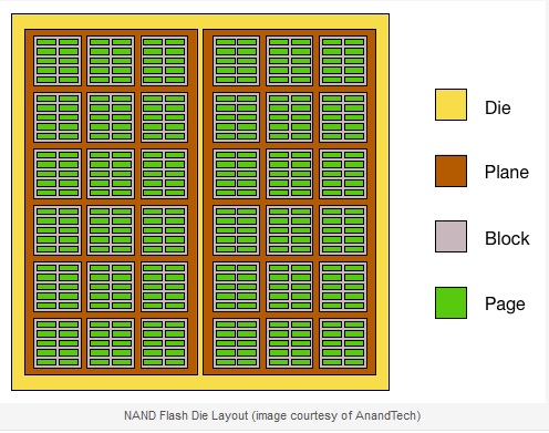
Actually on a byte basis, erasing is faster than programming as you will see. This is a simplified layout of a NAND memory, with two dies:
Pages are typically 8-16 KB in size, while blocks are much bigger, 4-8 MB in size. Programming can be done on a page basis, but erasing can only be done on a block basis. So when erasing, 500x (8 MB / 16 KB) cells are bring erased
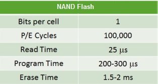
These are the typical times for doing various operations:
Erasing takes 6.67 (2000 µs / 300 µs) times as long as programming. But 500x time more cells are involved, so the real difference is 500x / 6.67x is 75x faster for erasing.
I don't know for sure but I would guess the difference is erasing is being done once with one command over 8 MB block, whereas programming is being done 500x to match the same number of bytes, and the time to send the commands plus the setup time inside the chip make account for the difference.
-
\$\begingroup\$ It takes more time to erase because going from 0 to 1 (or x to 1) takes more time than writing, going from 1 to 0 (or 1 to x). \$\endgroup\$– user338146Commented Aug 13, 2023 at 16:44
- NOR flash memory cell size is larger than NAND, therefore you have larger capacitance which leads to larger delay to charge/discharge the floating-gate (FG) of MOSFET via Fowler–Nordheim tunneling.
- NOR flash needs a "pre-program" before the erase to avoid "over-erased" cells. This "pre-program" process is time consuming. The "pre-program" refers to the operation of checking the existing data bits and programming any bits from the '1' (erase) state to the '0' (program) state. In NAND flash memory, the cells are connected in series inside a P-well substrate. Therefore, we can erase (storing 1) all those cells in bulk by applying elevated erasing voltage to P-well (e.g., +20v) and erase the whole block. This is not possible in NOR flash as NOR cells are in parallel and one need to erase them byte by byte (bit erasing is also possible).


